How to Design RF PCB and Material Selection?
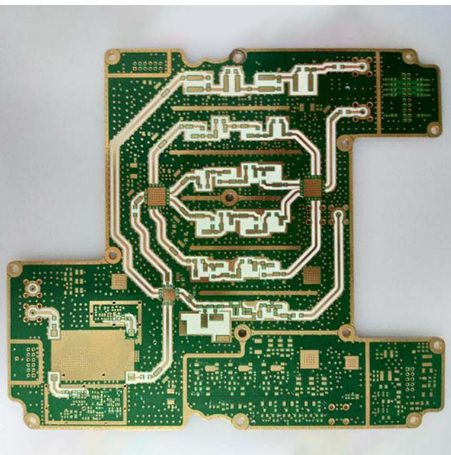
RF printed circuit boards are a highly complex but rapidly growing segment of the PCB manufacturing industry. In the PCB industry, boards that operate at frequencies above 100MHz are classified as RF PCBs. However, this standard stops at 2GHz. In addition, any board that operates at frequencies above 2GHz is called a microwave board. RF PCBs have components that work using radio frequencies. RF PCBs are a special category in the PCB manufacturing industry and are estimated to be the fastest growing sector.
What are Microwave Oven PCBs?
Any RF circuit board that operates at frequencies above 2GHz is a microwave PCB. The radio frequency at which it operates is the key difference between RF PCBs and microwave PCBs.
Any application that needs to receive and send radio signals uses RF PCBs, and microwave PCBs are used to transmit communication signals. Radar stations and mobile phones are two examples of typical applications of RF PCBs.
Different types of materials used to manufacture RF PCBs
Ceramic filled PTFE composites
They have excellent mechanical and electrical stability. Rogers RO3000 Series circuit materials offer consistent mechanical properties regardless of the dielectric constant (Dk) chosen, enabling multilayer board designs using a wide range of dielectric constant materials without warping or reliability issues. Unlike hydrocarbon-based competitors, Taconic RF Series offers low dissipation factor and high thermal conductivity potential, resisting oxidation, yellowing, dielectric constant rise, and dissipation factor drift.
Glass-Reinforced PTFE Laminates
They are more dimensionally stable than chopped fiber reinforced PTFE composites and are made from very light woven glass fibers. The materials in Taconic TL products have low dissipation factors, making them ideal for millimeter wave antennas and 77 GHz radar applications.
Hydrocarbon Ceramic Laminates
Manufacturers use them for microwave and millimeter wave frequency designs due to their lower loss and leaner nature than traditional PTFE materials. Rogers RO4000 products offer above-average thermal conductivity and a wide range of DK values (2.55–6.15). (.6-.8).
Thermoset Microwave Laminates
These materials offer good mechanical reliability, thermal expansion coefficients matched to copper, and low thermal coefficients of dielectric constant (Dk). High-frequency laminates manufactured by Rogers TMM are ideal for stripline and microstrip applications requiring high reliability.
Other Types of Materials
Ultra-Low Loss, High Heat, Halogen-Free Megtron 6
These boards are made from hydrocarbon resin-based MEGTRON 6, which is suitable for high-density interconnect (HDI) and high-speed (above 3 GHz) structures due to its high glass transition temperature (Tg) and low expansion.

Filled PTFE (random glass or ceramic)
Composite laminates, such as Rogers RT/duroid® high-frequency circuit materials, are selected for space applications due to their low electrical losses, low moisture absorption, and low outgassing properties.
Factors Affecting RF PCB Design
Matched Impedance
Maximum power transfer from source to load without distortion occurs in controlled impedance RF circuits when the impedance is constant along the trace. This impedance is the characteristic impedance (Z0) of the trace. In addition, the trace geometry, such as trace width, dielectric constant of the PCB material, trace thickness, and height from the reference ground plane, all affect the characteristic impedance. In addition, matching circuits are created to match these impedances.
Board Materials
RF PCB production involves specific materials that meet the needs of high-frequency operation. These materials should absorb a lot of heat, have low signal losses, and remain stable during high-frequency operation. Consistency over a wide frequency range is also an essential requirement for dielectric constant (DK), loss tangent (tan), and coefficient of thermal expansion (CTE) measurements. For these boards, the typical dielectric constant range is 3 to 3.5. For the frequency range of 10-30GHz, the loss tangent values are in the range of 0.0022 to 0.0095. In addition to these specific requirements, it is also important to consider material cost and simplicity of manufacturing.
Commonly used materials include those made of PTFE (polytetrafluoroethylene), ceramics, and hydrocarbons combined with glass. Rogers materials are commonly used for RF circuit boards. There are several versions of Rogers’ book. Here is a list of some of them:
Rogers TMM
RO 3000
RO 4000
RT/duroid
RF PCB Stack-up
When stacking up an RF board, details such as isolation between traces and components, power supply decoupling, number of layers and their arrangement, placement of components, etc. must be considered. The top layer is where the traces and RF components are placed. The ground plane and power plane follow closely, followed by the traces and non-RF parts. This configuration minimizes interference between RF and non-RF components. The ground return has a minimal path provided by the nearby ground plane. In summary, this stack-up works well for compact RF boards.
RF Trace Design
RF traces propagate high frequency signals, which makes them susceptible to transmission loss and interference issues. The main concern of the designer is the characteristic impedance of the trace. Traces on an RF board are considered as transmission lines. Coplanar waveguide (CPWC), microstrip, and stripline transmission lines are the three most commonly designed types of transmission lines. The RF trace design factors that affect proper operation and minimum loss are as follows:
- The length of the trace should be kept as short as possible to reduce attenuation.
- In layout, RF and normal traces must never be parallel. If placed like this, interference will occur between the two.
- Ground planes are required to provide a safe return path.
It is forbidden to place test points on the trace. The impedance matching value of the trace will be interrupted. The performance of the trace can be improved by making gradual bends instead of continuous sharp turns.
Designing the Ground Plane
- Any trace or component used in RF technology requires a return path for the current to flow.
- The ground plane takes care of this. However, the ground plane requires some additional design factors. Let’s look at these factors now.
- Each RF layer should have a separate ground plane. This ground plane is located directly below the layer to make the current flow path as short as possible.
- There should be no breaks in the ground plane. No breaks are allowed.
- Each shunt element used in the RF transmission line requires at least two ground vias, as these breaks can provide a shorter path for the current to return.
Via Design
RF traces should avoid vias as much as possible. Consider choosing a specific width and length based on the requirements. Vias cause parasitic capacitance in the board. This capacitance affects the high frequency operation of the RF board. Therefore, it is crucial to keep the following guidelines in mind when constructing vias to minimize interference from these frequencies:
- Increase the number of parallel vias to reduce parasitic capacitance.
- Each component pin or pad must have a dedicated via.
- Use stitching to implement ground planes where appropriate. This way, the ground return path for the current is shortened.
- Minimize the vias used in routing RF traces between layers.
- Use as many vias as the design allows to connect the inner layer planes and the top layer ground plane. Also, the distance between these vias should not exceed 1/20 of the signal wavelength.
Decoupling Power Supply
Using this method, the noise entering the circuit from the power supply is filtered out. Decoupling capacitors are the type of capacitors used for this purpose. These capacitors are connected to the power supply. Every RF circuit board must have impedance matching. Therefore, the impedance of the entire circuit should not change after the decoupling capacitors are connected. To prevent impedance changes, adopt the following design guidelines:
For decoupling, always connect capacitors with the lowest possible impedance.
To create the minimum impedance, run the capacitor at its self-resonant frequency (SRF). The SRF value of a capacitor is inversely proportional to its capacitance value.
Choose capacitors with an SRF close to the noise frequency.
Placement of Decoupling Capacitors
A successful RF design also depends on the placement of the decoupling capacitors. A short circuit is provided below, which shows two decoupling capacitors connected in parallel with an IC component.
The role of the higher capacitor is to store energy and filter out low-frequency noise from the system, while the lower capacitor filters out high-frequency noise.
Other rules related to placement include:
Components and decoupling capacitors should be on the same layer.
Arrange the capacitors parallel to the signal direction.
Reserve separate ground vias for each capacitor.
Capacitors should be arranged sequentially in the order of power supply capacitance. Therefore, the component with the lowest capacitance is closest to the power supply.
It is safe to say that RF PCBs can make a significant contribution to future communications. Manufacturers use these PCBs extensively in communication devices such as mobile phones. Learning to make RF PCBs is very beneficial and is one of the leading areas of the PCB industry.


