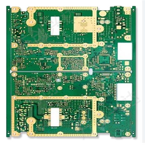
How to Design PCBs Efficiently and Minimize Errors
PCB design is a critical, time-consuming task. Any errors require engineers to meticulously check the entire design, analyzing each network and component. This process requires a level of carefulness comparable to chip design.
Typical PCB Design Process
The typical PCB design process consists of several steps, with the first three steps taking the most time. Schematic checking, for instance, is a manual process, which becomes overwhelming when dealing with complex designs, such as a System on Chip (SoC) circuit board with thousands of connections. Manually verifying each connection is tedious, and checking every single one is nearly impossible. This often leads to errors like incorrect connections, floating nodes, and more.
Common Issues in the Schematic Capture Stage:
- Case sensitivity: For example,
VDDEvs.vdde - Underscore errors: For example,
APLLVDDvs.APLL_VDD - Spelling mistakes
- Signal short-circuits
- Other design mistakes
To avoid these errors, it’s crucial to have a method for quickly checking the entire schematic. One effective way to do this is schematic simulation, though it is not commonly used in traditional PCB design. Schematic simulation allows you to observe the output results at the required nodes and automatically check for connection problems.

Example: Reducing Errors and Improving Efficiency
Consider a typical block diagram of a circuit board:
Figure 1: Block diagram of a typical circuit board
In complex designs, the number of connections can reach thousands. A small change in one part of the design can waste significant time checking the connections manually. With schematic simulation, however, designers can quickly identify connection issues, saving time and reducing errors.
Using Schematic Simulation for Checking
In schematic simulation, a testbench is created where stimulus signals are applied to the required inputs. The output results are observed at specific signal points of interest. Probes are connected to the nodes being observed, and the voltages and waveforms at those nodes indicate whether the schematic has errors.
Figure 2: Some signals of a typical device under test (DUT)
In the schematic, various modules like regulators, operational amplifiers (op-amps), etc., are used to adjust the signals, such as a power supply signal obtained via a regulator.
Figure 3: Schematic diagram of the sample circuit board
By performing schematic simulation, you can verify the entire design for correctness. Stimulus signals are applied, and the resulting output values are observed, confirming the accuracy of the design.
Figure 4: Schematic testbench and simulation values of each node
By carefully adjusting stimulus signals or component values, you can explore design changes and ensure that the connections are correct. This automatic checking of connections saves significant time and increases the chances of catching design errors early.
Advantages of Schematic Simulation
- Time Efficiency: Schematic simulation can identify errors and verify connections in a matter of seconds, significantly reducing design time.
- Error Detection: By using simulation, you can catch common issues like wrong connections, floating nodes, and incorrect signal paths before production.
- Design Exploration: It allows for easy testing of design changes, ensuring that alterations do not introduce new errors or issues.
- Improved Design Quality: Simulation increases the chances of achieving a correct design on the first try, reducing the need for costly revisions and rework.
Incorporating schematic simulation into the PCB design process not only saves valuable time but also increases the accuracy and efficiency of the entire workflow. By automating the process of checking for errors and verifying connections, designers can improve the overall quality of the PCB and minimize the chances of issues in the final design.


