How to Design a 2-Layer Flex PCB
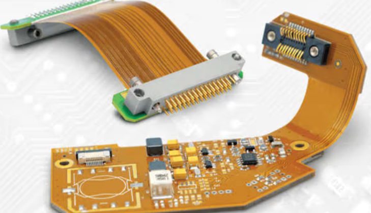
Flexible PCBs (printed circuit boards) provide the ability to bend and conform to various shapes, making them an essential technology for space-constrained and dynamic applications. A 2-layer flex PCB contains a flexible dielectric layer sandwiched between two conductive copper layers. Designing these PCBs requires unique considerations, including material selection, layout techniques, manufacturability, and reliability.
This guide outlines a step-by-step process for designing a 2-layer flex PCB, with a focus on the critical aspects to consider.
Design Process Overview
The typical workflow for designing a 2-layer flex PCB involves the following steps:
- Define circuit requirements and interfaces
- Choose a flex material stackup
- Create a circuit schematic
- Plan layout and component placement
- Route traces and place vias
- Specify flex outlines and bend regions
- Add annotations and markers
- Review design rules and tolerances
- Verify electrical constraints
- Export Gerber and CAD files
Flexible Materials for 2-Layer PCBs
- Flexible Dielectric
- Material: Polyimide (PI) is the most common choice, offering excellent flexibility, heat resistance, and chemical stability.
- Thickness: Typically ranges from 25µm to 100µm.
- Copper Foil
- Type: Rolled annealed (RA) copper provides better flexibility.
- Thickness: Commonly 18µm to 35µm, chosen based on current-carrying requirements.
- Adhesive
- Used to bond copper foil to the dielectric.
- Acrylic or epoxy adhesives ensure durability under flexing.
- Cover Layer
- Polyimide or acrylic serves as a protective cover for the circuitry.
- Cutouts are included for pads and connections.
- Solder Mask
- Protects copper traces from environmental damage and short circuits.
Stackup Selection for 2-Layer Flex PCBs
A typical 2-layer flex PCB stackup includes:
- Core: Flexible dielectric (25µm–100µm)
- Layer 1 and 2: Rolled annealed copper foil (18µm–35µm)
- Cover: Polyimide or acrylic (25µm–50µm)
Trade-offs:
- Thinner cores allow smaller bend radii but limit current capacity.
- Thicker copper increases durability but reduces flexibility.
Schematic Design Considerations
When creating the circuit schematic:
- Define all component interfaces, connectors, and signal types.
- Mark rigid and flex regions explicitly.
- Highlight high-speed and critical signal paths.
- Include test points for debugging and verification.
Key Layout Considerations for 2-Layer Flex PCBs
- Component Placement
- Use only low-profile surface-mount components.
- Place components on rigid areas; avoid bends.
- Ensure even distribution to minimize stress concentration.
- Trace Routing
- Avoid sharp 90° turns; use 45° angles for better flexibility.
- Leave slack in traces near bends to accommodate movement.
- Route critical signals on inner layers for protection.
- Bend Areas
- Define bend regions with adequate bend radius to avoid trace cracking.
- Route traces perpendicular to the bending direction to minimize stress.
- Stiffeners
- Add stiffeners (e.g., FR4 or metal) near connectors, narrow flex segments, or large components for support.
- Test Points
- Include easily accessible test points on critical nets for debugging.
Design Rules for 2-Layer Flex PCBs
- Bend Radius: Maintain a minimum bend radius exceeding material specifications to prevent damage.
- Trace Width and Spacing: Ensure adequate width for current capacity and spacing to avoid shorts or crosstalk.
- Annular Rings: Ensure sufficient clearance between pads and via walls to avoid opens.
- Via Coverage: Use capped or filled vias to enhance durability.
- Test Point Dimensions: Provide safe probing access.
Manufacturing and Assembly Considerations
- Fabrication Steps
- Imaging: Photolithography transfers the circuit layout.
- Etching: Removes excess copper to form traces.
- Die Cutting: Shapes the flex PCB outline and bend regions.
- Cover Lamination: Adds protective layers to the circuitry.
- Assembly Guidelines
- Assemble components only on rigid sections.
- Use adhesives or stiffeners for additional support during assembly.
- Opt for SMT assembly techniques for precise component placement.
- Conformal Coating (Optional):
- Apply acrylic, silicone, or epoxy coatings for enhanced durability.
Design Verification Checklist
- Verify all electrical clearances and constraints.
- Ensure trace widths meet current requirements.
- Check impedance for high-speed traces.
- Validate bend radius and ensure it meets material specifications.
- Confirm no components are near bend areas.
- Test prototypes for dynamic durability and flexibility.
Designing a reliable 2-layer flex PCB requires meticulous attention to material selection, layout, and manufacturability. By adhering to the outlined guidelines, engineers can create flex PCBs that meet functional, mechanical, and quality requirements for modern applications.
KKPCB conducts research on special processing technologies such as ordinary double-sided boards, thick copper circuit boards, high-frequency circuit boards, HDI circuit boards, rigid-flexible circuit boards, FPC flexible boards, buried blind hole circuit boards, and IC carrier boards. Provides PCB design, PCB layout, PCB prototyping and PCB assembly services.


