How to Create Vias on High-Frequency PCBs
Vias are essential in multi-layer PCBs, enabling interconnections between different layers. However, their impact on signal integrity and manufacturing costs cannot be overlooked. Drilling costs often account for 30-40% of total PCB production expenses. This guide explains via types, their effects on high-frequency signals, and best practices to minimize negative impacts.
What is a Via?
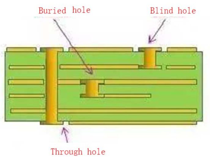
A via is a small hole on a PCB that connects different layers electrically. Structurally, a via consists of a drill hole and a pad. Vias are classified into three types based on their function and placement:
- Blind Vias:
- Connect external layers to internal layers.
- Do not pass through the entire board.
- Common in HDI (high-density interconnect) PCBs.
- Buried Vias:
- Connect only internal layers.
- Invisible on the external layers.
- Typically used in complex, high-layer PCBs.
- Through-Hole Vias:
- Pass through the entire PCB.
- The most common type, offering simplicity and cost-effectiveness.
Via Parasitics in High-Frequency Designs
Parasitic Capacitance
The via has inherent stray capacitance that affects signal quality by slowing rise times. The parasitic capacitance of a via is given by:
C=1.41⋅ε⋅T⋅D1D2−D1C = \frac{1.41 \cdot \varepsilon \cdot T \cdot D_1}{D_2 – D_1}C=D2−D11.41⋅ε⋅T⋅D1
Where:
- ε\varepsilonε: Dielectric constant of the PCB material.
- TTT: PCB thickness.
- D1D_1D1: Diameter of the via pad.
- D2D_2D2: Diameter of the solder mask opening.
Example: For a 50mil PCB thickness, D1=20milD_1 = 20milD1=20mil, D2=40milD_2 = 40milD2=40mil, and ε=4.4\varepsilon = 4.4ε=4.4:
C=1.41⋅4.4⋅0.050⋅0.0200.040−0.020=0.31 pFC = \frac{1.41 \cdot 4.4 \cdot 0.050 \cdot 0.020}{0.040 – 0.020} = 0.31\ \mathrm{pF}C=0.040−0.0201.41⋅4.4⋅0.050⋅0.020=0.31 pF
This capacitance can increase the rise time, affecting high-speed signal transmission.
Parasitic Inductance
The via also introduces parasitic inductance, which is more detrimental in high-speed designs. The inductance of a via is given by:
L=5.08⋅h⋅[ln(4hd)+1]L = 5.08 \cdot h \cdot \left[ \ln{\left(\frac{4h}{d}\right)} + 1 \right]L=5.08⋅h⋅[ln(d4h)+1]
Where:
- LLL: Inductance (nH).
- hhh: PCB thickness (via length).
- ddd: Drill hole diameter.
Example: For a 50mil PCB thickness and 10mil drill diameter:
L=5.08⋅0.050⋅[ln(4⋅0.0500.010)+1]=1.015 nHL = 5.08 \cdot 0.050 \cdot \left[ \ln{\left(\frac{4 \cdot 0.050}{0.010}\right)} + 1 \right] = 1.015\ \mathrm{nH}L=5.08⋅0.050⋅[ln(0.0104⋅0.050)+1]=1.015 nH
This inductance can introduce impedance to high-frequency signals.
Best Practices for Via Design in High-Frequency PCBs
- Optimize Via Size:
- Use smaller vias for signal traces to minimize parasitic capacitance and inductance.
- Employ larger vias for power and ground connections to reduce impedance.
- Minimize PCB Thickness:
- Thinner boards reduce via parasitics and improve signal performance.
- Avoid Unnecessary Vias:
- Limit the number of vias in signal paths to reduce discontinuities.
- Close Proximity for Power and Ground Pins:
- Place power and ground pins close together to minimize lead length and inductance.
- Add Ground Vias:
- Introduce additional ground vias near high-frequency signal traces to reduce noise and improve return paths.
- Use Microvias for HDI Boards:
- For high-density designs, microvias (via diameter ≤ 6mil) improve performance and save space.
- Microvias can be drilled directly on pads, improving signal integrity.
Impact of Vias on Signal Integrity
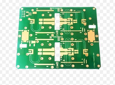
Vias cause impedance mismatches in high-speed signals, leading to reflections. The reflection coefficient of a via is:
R=Zv−Z0Zv+Z0R = \frac{Z_v – Z_0}{Z_v + Z_0}R=Zv+Z0Zv−Z0
Where ZvZ_vZv is the via impedance and Z0Z_0Z0 is the trace impedance.
For a typical 50-ohm line:
- A 6-ohm decrease in impedance due to the via results in a reflection coefficient of:
R=44−5044+50=−0.06R = \frac{44 – 50}{44 + 50} = -0.06R=44+5044−50=−0.06
While minor, cumulative reflections from multiple vias can degrade performance in high-speed designs
Vias are integral to high-frequency PCBs, but their parasitic effects must be carefully managed. By optimizing via size, placement, and type, designers can minimize negative impacts and ensure reliable performance in high-speed circuits. When designing for advanced applications, adopting HDI techniques like microvias and reducing PCB thickness can further enhance signal integrity and overall performance.
KKPCB conducts research on special processing technologies such as ordinary double-sided boards, thick copper circuit boards, high-frequency circuit boards, HDI circuit boards, rigid-flexible circuit boards, FPC flexible boards, buried blind hole circuit boards, and IC carrier boards. Provides PCB design, PCB layout, PCB prototyping and PCB assembly services.


