How to Check for PCB Warpage: Techniques and Methods
Key Takeaways
- Stress during fabrication, such as thermal expansion and contraction, imbalanced copper distribution, and improper handling, can lead to warpage.
- Utilize tools like feeler gauges, height gauges, contour gauges, optical profilometers, and Finite Element Method (FEM) simulations to accurately measure PCB warpage.
- Effective design practices using OrCAD X, such as symmetrical component placement and proper copper distribution, combined with precise fabrication controls, can significantly reduce the risk of PCB warpage.
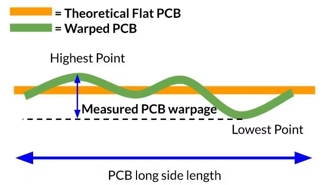
How to measure PCB warpage by measuring.
Warpage is often caused by stress during the PCB construction process when the board undergoes expansion and contraction, leading to internal stress that results in warpage. Learning how to detect PCB warpage early in the assembly stage is crucial because it can impact printing, mounting, and soldering processes.
Warpage can cause various problems, such as component misalignment, poor solder joint quality, and device failure. The change in flatness is due to the thermal expansion or contraction of board materials, resulting in micro-level strains and deformations that affect the placement of SMT components. Below, we explain methods of how to check PCB warpage and calculation methods for adherence to standards.
How to Check PCB Warpage
| Method | Description | Usage for Checking PCB Warpage |
| Feeler Gauge Method | Uses feeler gauges to measure warpage between high and low points. Good for large warpage values. | Simple method to check for significant warpage by manually inserting gauges between points on the PCB surface. |
| Height Gauge | Measures height difference between high and low points accurately in inches or millimeters. | Provides precise measurements at specific points, useful for detailed inspection and quality control. |
| Contour Gauge | Traces the profile of a warped PCB, providing a complete shape mapping. | Offers a visual representation of the PCB surface, highlighting all high and low points for comprehensive analysis. |
| Optical Profilometer | Projects light onto PCB, capturing an image to generate a precise 3D profile map. | Delivers highly accurate and detailed 3D surface maps, ideal for advanced diagnostics and identifying warpage patterns. |
| Finite Element Method (FEM) | Provides precise warpage measurements; higher precision tools offer better accuracy. | Uses simulation to predict warpage behavior, useful for design validation and preemptive adjustments. |
Characterizing PCB Warpage
Warpage is determined on a flat surface and represents the maximum height difference from the lowest to the highest point across the board length. Major IPC standards are associated with warpage, and are separated into warpage classes outlined below.
- IPC-6011: Generic Performance Specification for Printed Circuit Boards
- IPC-6012: Qualification and Performance Specification for Rigid Printed Boards
How to Check PCB Warpage as a Percent
Manufacturers need to define the appropriate IPC class for their PCBs based on the specific application and required reliability. These standards offer a clear benchmark for suppliers to adhere to. Warpage is measured on a flat surface and indicates the maximum height difference between the lowest and highest points across the board’s length, as shown on the initial diagram.

Different Classes of Warpages With Maximum Allowance
| Class | Maximum Warpage Allowance | Example for 500 mm PCB | Usage |
| Class 1 | Up to 0.2% (0.2 mm per 100 mm) of PCB length warpage | Warpage up to 1.0 mm | General-purpose boards |
| Class 2 | Up to 0.15% of PCB length warpage | Warpage up to 0.6 mm | Intermediate reliability requirements |
| Class 3 | Up to 0.1% of PCB length warpage | Warpage up to 0.5 mm | Higher reliability applications |
| Class 4 | Up to 0.05% of PCB length warpage | Warpage up to 0.25 mm | Most restrictive, critical applications |
- For general-purpose boards (Class 1), up to 0.2% warpage is acceptable.
- For higher reliability applications (Class 3 or 4), a warpage of 0.1% or less is recommended.
Sources of Warpage
PCB warpage can occur from a variety of different sources. Below, we’ve summarized some key causes.
| Factor | Description |
| During Lamination | The lamination process involves bonding multiple layers of copper and dielectric materials under heat and pressure. Warpage can occur due to thermal mismatch, unequal pressure distribution, and uneven resin flow. |
| During Hot Air Solder Leveling | The tin furnace is heated to 225℃-265℃ for 3-6 seconds. The board undergoes sudden heating and cooling, leading to thermal stress, warping, and distortion. |
| During Baking | Baking PCBs at around 150°C can activate stresses from lamination, causing warpage, especially in PCBs with lower glass transition (Tg) materials. High elasticity of resins above Tg point makes them prone to deformation. |
| Improper Handling and Stacking | Mishandling and improper stacking during processing and storage can apply mechanical stresses, leading to warpage, especially in thinner PCBs. |
| Imbalanced Copper Distribution | Uneven copper distribution causes uneven expansion and contraction during heating and cooling, leading to warpage. Proper copper balancing during design helps minimize this. |
| Material Incompatibility | Mismatching materials with different properties can cause uneven expansion during heating and cooling, leading to warpage. The orientation of glass fibers in prepregs also affects warpage. |
| Improper Process Controls | Uneven or excessive heating during fabrication can exacerbate warpage by activating more stresses. Controlling process temperatures and times helps minimize this. |
| Storage Conditions | Improperly secured or stacked PCBs during storage can lead to mechanical stresses and warpage, especially in thinner PCBs. |
| Board Size and Number of Panels | Large PCBs with broad sections hanging between chains in back weld furnaces are at higher risk of warping due to weight distribution. |
Preventing PCB Warpage With OrCAD X
Component misalignment due to warping can hinder the proper installation of the board into the chassis or socket within the device, ultimately affecting the normal operation of the entire subsequent process. Warpage can be prevented through two methods:
- Good design prior to fabrication.
- Reliable PCB fabrication steps.
Design-Related Methods Enabled by OrCAD X
| Aspect | Description | How OrCAD X Helps You in These Aspects |
| Component and Copper Distribution on Board | Ensures symmetrical arrangement of interlayer prepregs and similar area of circuit patterns on both sides of the board to prevent warping. | 3DX engine for viewing components as they would appear on the board.Allows for verifying placement and arrangement, ensuring symmetrical designs.Stackup editor ensures a balanced copper distribution through symmetry and a consistent layer thickness throughout. |
| Proper Design | Balances copper areas and lines on each side, and uses symmetrical arrangement of prepregs. | Constraint-driven routing in OrCAD X helps manage copper balance. Real-time DRCs ensure rule adherence. |
| Reduction of Board Size and Number of Panels | Smaller boards or using the long side as the edge on the chain to distribute weight and reduce warping. | OrCAD X has design tools to allow adjustment of board size and shape to meet manufacturing constraints. |
| Copper Shape Management | Tools for creating and managing copper shapes, such as ground and power planes, including shape merging and Z Copy method. | Allows for fine customization of large copper planes, reducing localized stresses that can lead to bowing and flexing.Allows customization of how a shape pour is filled – from solid, crosshatch, diagonal, and horizontal.Allows for fine-tuning copper areas affecting capacitance and thermal distribution. |
| Package-to-Package Spacing Check | Organizes symbols into classes and applies specific spacing rules. | Prevents crowding and stress between components, reducing the risk of warping.Aids in better distribution of components throughout the board. |
| Via Under Component Check | Checks for vias placed under components. | Avoids vias under components, reducing the risk of stress points and potential flexing. |
| Through-Hole Pins Under SMD Component Check | Checks for through-pins incorrectly positioned under components on the opposite side. | Prevents placement conflicts that could introduce mechanical stress and warping. |
| Same Net Spacing Checks | Offers advanced checks for same-net connections across different vias and layers. | Ensures uniform current distribution and reduces thermal stress, minimizing the risk of warping. |
| Cline Width vs. Padstack Width Check | Checks trace width against pad width to avoid excessive trace widths connecting to pads. | Ensures proper trace-to-pad connections, reducing mechanical stress that could cause bowing and flexing. |
Fabrication Related Methods A Manufacturer Uses to Minimize PCB Warpage
| Fabrication Related Methods | Details |
| The Latitude and Longitude of the Prepreg | Align prepreg (warp direction: rolling direction; weft direction: width direction) to prevent warping. |
| Using Router Instead of V-Cut Dividers | Use a router instead of V-cut dividers to maintain structural integrity and prevent warping. |
| Stress Relief After Lamination | Place boards flat in an oven at 150°C for four hours to gradually release stress and fully cure resin. |
| Thin Plate Straightening During Electroplating | Use special clamping rollers for ultra-thin boards (0.4 to 0.6mm) to prevent deformation after plating. |
| Cooling After Hot Air Leveling | Place boards on a flat surface for natural cooling. Avoid submerging in cold water; use air flotation beds. |
| Treatment of Warped Boards | Bake warped boards at 150°C under heavy pressure for 3-6 hours, then cool naturally under pressure. Multiple rounds may be needed. |
| Flatness Check During Final Inspection | Perform 100% flatness checks. Bake unqualified boards at 150°C under heavy pressure for 3-6 hours and cool naturally under pressure. |
| Handling During Electroplating | Use special clamping rollers for ultra-thin multi-layer boards to prevent warping. |
| Plate Flattening | Use specialized machines to flatten boards during manufacturing, though results may vary. |
| Addressing Environmental Factors | Store substrates with moisture-proof packaging and minimize humidity in warehouses. |
| Thermal Management | Bake and dry boards appropriately before and after lamination. Cool naturally after hot air leveling. |
| Pallets and Fixtures | Reduce board size or use the long side as the edge on chains during back weld furnaces to distribute weight and reduce warping risk. |
| Use a Tray Jig or Reflow Carrier | Support boards during soldering with a tray jig or reflow carrier to prevent warping during heating and cooling cycles. |
Now that you’ve learned how to check PCB warpage, ensure you create a reliable board to minimize warpage
KKPCB provides global customers with one-stop services from PCB layout, prototype PCB proofing, PCB manufacturing, PCBA processing (including SMT and DIP), PCBA testing, PCBA product assembly and outbound packaging. You could provide a Gerber file or BOM list to us, we will offer the finished PCB products or PCB assembly which are satisfied with you.


