


How to Check for PCB Warpage: Techniques and Methods
PCB warpage is a common issue caused by stress during the PCB construction process, where the board undergoes expansion and contraction, leading to internal stress and deformation. Detecting PCB warpage early in the assembly stage is crucial, as it can negatively impact printing, mounting, and soldering processes. Warpage can lead to problems such as component misalignment, poor solder joint quality, and device failure. Below, we explore techniques to check for PCB warpage, calculation methods, and strategies to minimize it.
How to Check PCB Warpage
Several methods are available to measure PCB warpage, each suited for different levels of precision and application requirements.
| Method | Description | Usage for Checking PCB Warpage |
|---|---|---|
| Feeler Gauge Method | Uses feeler gauges to measure warpage between high and low points. | Simple method for detecting significant warpage by manually inserting gauges between PCB points. |
| Height Gauge | Measures height differences between high and low points in inches or millimeters. | Provides precise measurements at specific points, ideal for detailed inspection and quality control. |
| Contour Gauge | Traces the profile of a warped PCB, providing a complete shape mapping. | Offers a visual representation of the PCB surface, highlighting all high and low points. |
| Optical Profilometer | Projects light onto the PCB, capturing an image to generate a 3D profile map. | Delivers highly accurate 3D surface maps, ideal for advanced diagnostics and warpage pattern analysis. |
| Finite Element Method (FEM) | Uses simulation to predict warpage behavior. | Useful for design validation and preemptive adjustments during the design phase. |
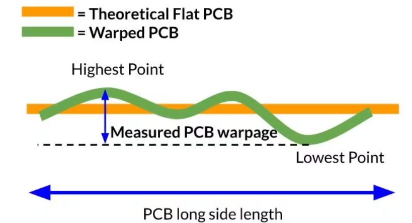
Characterizing PCB Warpage
PCB warpage is determined by measuring the maximum height difference between the lowest and highest points across the board’s length on a flat surface. Major IPC standards provide guidelines for acceptable warpage levels, categorized into different classes based on application requirements.
IPC Standards for PCB Warpage
- IPC-6011: Generic Performance Specification for Printed Circuit Boards.
- IPC-6012: Qualification and Performance Specification for Rigid Printed Boards.
How to Calculate PCB Warpage as a Percent
Warpage is calculated as a percentage of the PCB’s length. For example, a 500 mm PCB with a 1.0 mm warpage has a warpage percentage of:Warpage %=(Warpage Height (mm)PCB Length (mm))×100Warpage %=(PCB Length (mm)Warpage Height (mm))×100
Different Classes of Warpage with Maximum Allowance
| Class | Maximum Warpage Allowance | Example for 500 mm PCB | Usage |
|---|---|---|---|
| Class 1 | Up to 0.2% (0.2 mm per 100 mm) | Warpage up to 1.0 mm | General-purpose boards with lower reliability requirements. |
| Class 2 | Up to 0.15% | Warpage up to 0.6 mm | Intermediate reliability applications. |
| Class 3 | Up to 0.1% | Warpage up to 0.5 mm | Higher reliability applications, such as automotive or industrial boards. |
| Class 4 | Up to 0.05% | Warpage up to 0.25 mm | Most restrictive, critical applications like aerospace or medical devices. |
Sources of PCB Warpage
PCB warpage can arise from various factors during manufacturing and handling. Below are the key causes:
| Factor | Description |
|---|---|
| During Lamination | Uneven pressure, thermal mismatch, or resin flow during lamination can cause warpage. |
| During Hot Air Solder Leveling | Sudden heating and cooling in tin furnaces (225℃-265℃) leads to thermal stress. |
| During Baking | Baking at 150°C activates stresses from lamination, especially in low-Tg materials. |
| Improper Handling and Stacking | Mechanical stresses from mishandling or improper stacking can deform PCBs. |
| Imbalanced Copper Distribution | Uneven copper layers cause uneven expansion and contraction during thermal cycles. |
| Material Incompatibility | Mismatched materials with different thermal properties lead to uneven expansion. |
| Improper Process Controls | Uneven or excessive heating during fabrication exacerbates warpage. |
| Storage Conditions | Improperly secured or stacked PCBs during storage can lead to mechanical stress. |
| Board Size and Number of Panels | Large PCBs or panels with uneven weight distribution are prone to warping. |
Fabrication Methods to Minimize PCB Warpage
Manufacturers employ several techniques to reduce PCB warpage during fabrication:
| Method | Details |
|---|---|
| Align Prepreg Layers | Align prepreg warp and weft directions to prevent uneven expansion. |
| Use Routers Instead of V-Cut Dividers | Routers maintain structural integrity better than V-cut dividers. |
| Stress Relief After Lamination | Bake boards at 150°C for four hours to release stress and cure resin. |
| Thin Plate Straightening | Use clamping rollers for ultra-thin boards (0.4 to 0.6 mm) during plating. |
| Cooling After Hot Air Leveling | Cool boards naturally on flat surfaces; avoid cold water immersion. |
| Baking Warped Boards | Bake warped boards at 150°C under heavy pressure for 3-6 hours. |
| Flatness Checks During Final Inspection | Perform 100% flatness checks and re-bake unqualified boards. |
| Thermal Management | Bake and dry boards appropriately before and after lamination. |
| Use Tray Jigs or Reflow Carriers | Support boards during soldering to prevent warping during thermal cycles. |
Detecting and minimizing PCB warpage is essential for ensuring the reliability and functionality of electronic devices. By understanding the causes of warpage, employing accurate measurement techniques, and adhering to IPC standards, manufacturers can produce high-quality PCBs. Implementing fabrication best practices, such as proper material alignment, stress relief, and thermal management, further reduces the risk of warpage.
By following these guidelines, you can create reliable PCBs that meet the stringent requirements of modern electronics, ensuring optimal performance and longevity.
At KKPCB, we specialize in high-quality PCB assembly with advanced SMT, THT, and mixed technology, delivering precision, reliability, and performance for automotive, medical, aerospace, industrial, and consumer electronics. Our ISO 9001, IATF 16949, and IPC-A-610 certified facilities ensure rigorous quality control, including 100% AOI, X-ray, ICT, and functional testing, guaranteeing defect-free products. From prototypes to small and medium-volume production, we offer turnkey and consignment assembly services, ensuring efficient, cost-effective, and scalable manufacturing.