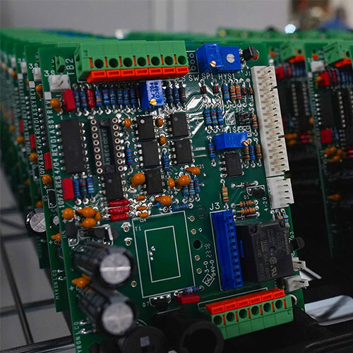
How to avoid radio frequency and microwave PCB design issues
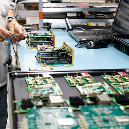
Modern PCB combines various digital and hybrid signal technology, so layout and design become more challenging, especially when RF and microwave mixed are used for subcutors. When viewing RF PCB, you need to consider some matters, whether you cooperate with us or other RF printing circuit board suppliers or design yourself.
First of all, the RF frequency range is usually 500 MHz to 2 GHz, but the design higher than 100 MHz is usually regarded as RF PCB. If you try more than 2 GHz, you are in the range of microwave frequency.
There are several main differences in the design of RF and microwave printing circuit boards that need to be considered -the difference between them and standard numbers or simulation circuits.
Simply put, the RF printing circuit board processing is essentially a very high -frequency analog signal. Your RF signal can reach any voltage and current level at almost any time, as long as it is at the minimum and maximum limit.
RF and microwave printing circuit boards run at specific frequencies and convey signals in a specific frequency band. The strip filter is used to transmit signals in the “target frequency band”, and any signal beyond this frequency range will be filtered out. The frequency band can be very narrow or wide, and can be transmitted through high frequency carrier waves.
Special materials and equipment
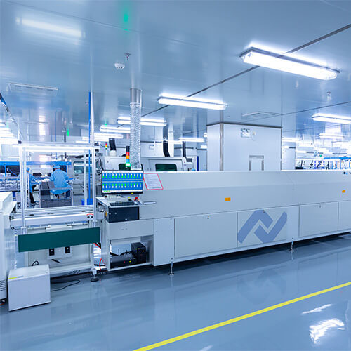
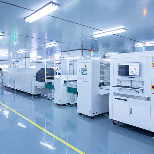
RF printing circuit board suppliers and manufacturers need the combination of standards and dedicated equipment for appropriate processing and manufacturing. Plasma etching machine is one of the more important requirements because it can maintain the high quality of the hole and minimize the deviation.
Laser direct imaging (LDI) device is also often used for RF circuits because it is better than traditional exposure tools. You need LDI background to ensure that the circuit board manufacturing maintains extremely tight width width and the requirements of the front and back.
Due to the sensitivity of the signal, especially compared with other digital signals, the radio frequency and microwave PCB using high -frequency layer pressure plates may be difficult to design.
Here are some matters that need to be considered to ensure that your design is efficient and to maximize the risk of failure, signal interruption and other invasion.
RF and microwave signals are very sensitive to noise -much more sensitive than high -speed digital signals. This means that you need to minimize the noise, bell, and reflection, and at the same time be careful to deal with the entire system.
Returning the signal with the least inductance -the ground floor below the signal will be easier to ensure this path.
Discipline matching is important. With the rise of RF and microwave frequency, the tolerance will become smaller. Generally, the PCB drive needs to be fixed, such as 50 ohms, which means that during the transmission and sending to the receiver, the drive outputs 50 ohms.
The transmission line that is curved due to wiring restrictions should use a curved radius that is at least three times larger than the central conductor width. This will minimize characteristic impedance.
It is necessary to minimize the return loss, whether it is reflected by the signal or the bell. There will always be a return path, but your design should guide it and prevent the return from multi -layer leakage through the PCB.
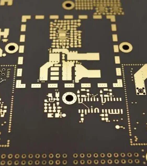
Use of high -frequency layer pressure plates
The layer pressure materials used to manufacture RF printing circuit boards add a layer of safety and protection to all your equipment. These materials can help your device process all three common thermal transmission types: transmission, convection and radiation.
Thermal management is the primary focus of all PCB applications in any industry, especially in the case of high frequency.
Finding a suitable high -frequency layer for PCB needs to find various characteristics and determine how to combine them into a picture. This is a complicated problem that you must weigh between multiple options and use cases.
You should choose them according to the degree of the high -frequency PCB layer pressure plate suitable for your application, and pay special attention to some important features:
Thermal expansion coefficient (CTE)
Dielectric constant (DK) and its thermal coefficient
Smooth copper/material surface contour
Thermal conductivity
thickness
Flexibility of the preservation circuit

