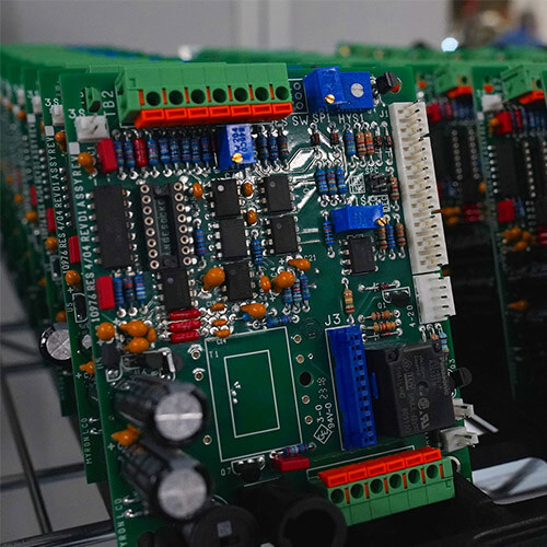
How to Avoid Creep on Board Assemblies
Creep is the slow, time-dependent deformation of materials under mechanical stress, which can lead to reliability issues in printed circuit board assemblies (PCBAs). It becomes particularly significant at elevated temperatures or under constant stress. In electronic assemblies, creep can cause solder joint failure, delamination, or component misalignment, particularly in high-reliability applications.
Here are guidelines and strategies to minimize creep in board assemblies:
1. Material Selection
a. PCB Substrate
- Use high-quality materials with low creep susceptibility, such as:
- High-performance laminates (e.g., FR-4, Rogers RT-duroid®).
- Thermal-stable substrates, like polyimide or ceramic-based materials, for high-temperature environments.
- Materials with lower coefficients of thermal expansion (CTE) are preferable to reduce stress during temperature cycles.
b. Solder Alloy
- Choose solder alloys with higher creep resistance:
- Lead-free options: SAC305 (Sn-Ag-Cu) or specialized high-temperature alloys like Sn-Cu-Ni.
- Traditional lead-based solder (Sn-Pb) offers good creep resistance but is less environmentally friendly.
c. Component Materials
- Opt for components and leads made from materials with similar thermal and mechanical properties as the PCB to minimize mismatch-induced stress.
2. Design Considerations
a. Proper Component Placement
- Distribute heavy or large components evenly across the board to prevent localized stress.
- Avoid placing high-mass components near board edges or unsupported regions.
b. Thermal Management
- Include adequate thermal reliefs, heat sinks, or thermal vias to dissipate heat and reduce the thermal gradient.
c. Hole Design
- Use plated through-holes with adequate wall thickness to enhance mechanical strength and minimize deformation.
- Ensure proper annular ring dimensions to provide robust solder joints.
3. Assembly Practices
a. Controlled Soldering Process
- Use precise temperature profiles to avoid overexposure of the solder and substrate to heat, which can accelerate creep.
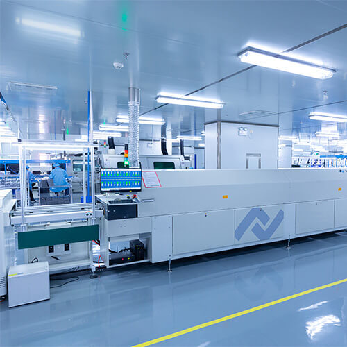
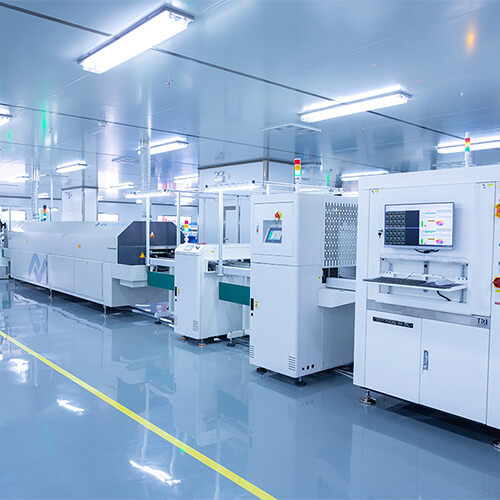
- Reflow soldering with optimized ramp-up, soak, and cooling phases minimizes thermal stress.
b. Reinforcement
- Use underfill materials for large or heavy components to distribute stress evenly and reduce creep potential.
- Apply corner staking or edge bonding for components subjected to vibration or mechanical load.
4. Mechanical Support
a. Board Stiffeners
- Add stiffeners or mechanical supports to reduce bending and flexing of the PCB.
b. Component Anchoring
- Use clips, adhesives, or brackets to secure heavy components and reduce stress on solder joints.
c. Enclosure Design
- Ensure the PCB is properly supported within the enclosure to prevent flexing during use.
5. Environmental Control
a. Minimize Thermal Cycling
- Design for environments with controlled and stable temperatures to reduce thermal cycling, which can induce creep.
b. Vibration Dampening
- Use vibration dampening mounts or enclosures to protect the assembly from mechanical stress.
6. Testing and Quality Assurance
a. Thermal Stress Testing
- Perform accelerated thermal cycling to evaluate creep resistance under expected operating conditions.
b. Mechanical Stress Testing
- Conduct vibration and mechanical load testing to identify weak points in the assembly.
c. Inspection
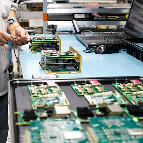
- Use X-ray or automated optical inspection (AOI) to detect early signs of creep, such as deformed solder joints or delamination.
7. Advanced Techniques
a. Use of Creep-Resistant Laminates
- High-performance laminates like PTFE-based composites (e.g., RT-duroid®) offer superior resistance to deformation at elevated temperatures.
b. Conformal Coatings
- Apply conformal coatings or potting compounds to reduce mechanical stresses and protect solder joints from environmental factors.
c. Stress Relief Designs
- Incorporate stress relief loops in the leads of through-hole components to accommodate thermal expansion and contraction.
By carefully selecting materials, optimizing design, adhering to best assembly practices, and conducting thorough testing, the risks associated with creep in PCB assemblies can be significantly reduced. These measures are especially critical for high-reliability applications such as aerospace, automotive, and medical devices.


