How PCB Solder Mask Works
What is PCB Solder Mask?
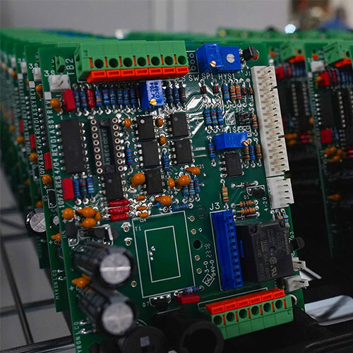
PCB solder mask is also known as PCB solder resist or PCB solder mask. It is a thin polymer protective layer PCB layer or coating that is applied on the copper traces to avoid initiating corrosion and oxidation processes after the PCB manufacturing process. It provides protection against many harmful factors. It is the most reliable way to limit this and extend the life of the PCB. It is very important in PCB.
This layer of coating permanently covers the entire circuit of our PCB, so in this way, we can extend the life of the PCB.
PCB solder mask process includes:
(i) Pretreatment
(ii) Coating
(iii) Drying
(iv) Prebaking
(v) Registration
(vi) Exposure
(vii) Development
(viii) Inspection
(ix) Final curing.
Application of PCB solder mask
Given below are some applications of PCB solder mask:
☆ Stop corrosion and oxidation processes on PCB.
☆ Reduce the amount of solder paste required for the soldering process.
☆ Increase the breakdown voltage of the dielectric material of the circuit board.
☆ Prevent environmental pollutants during processing.
☆ Extend the life of the PCB.
☆ Between the components of the circuit board, the insulation performance is improved.
☆ Prevent the generation of metal whiskers.
☆ Prevent the formation of solder bridges, which are unwanted connections on the PCB board. These solder bridges can cause short circuits on the board, resulting in damage.
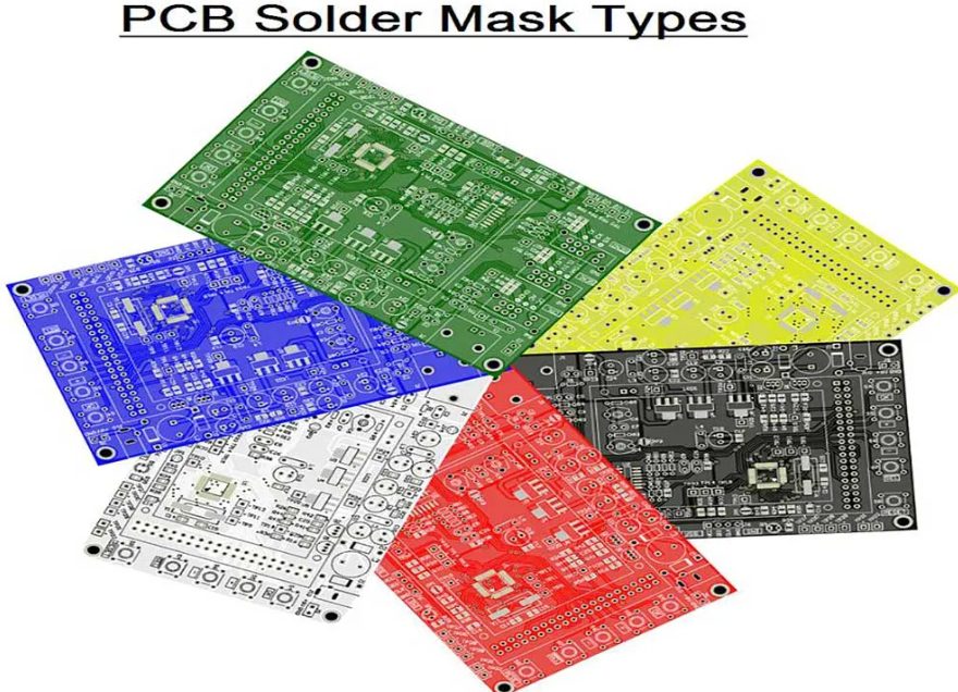
PCB Solder Mask Types
The most common types of PCB solder masks are as follows:
★ Epoxy Liquid Solder Mask
This is a cost-effective type of PCB solder mask. PCBs are screen printed with this solder mask. Screen printing is a printing process that creates an ink blocking pattern by using different types of grids. The grid allows for some open areas, which are determined for the ink transfer process. It has a high working efficiency.
★ Top and bottom masks
Most engineers use these PCB solder masks to identify the green mask openings that have been placed on the PCB. Through epoxy, we enable the application of this mask. Through multiple openings, on the board, the pins registered through these masks are connected. On the upper side, the traces are top traces and the mask is the top side (mask). On the other hand, on the bottom, the mask is called the bottom side (mask).
★ Liquid Photosensitive Mask
Liquid Photosensitive Mask
This mask is made of alkaline substances. It has two liquid mixtures. There is isolation between these liquids, but when the mask needs to be used, mixing (liquid) is done. Therefore, the service life is extended. Its main advantage is cost-effectiveness. This mask combines many polymers and other solvents.
No surface preparation procedures are required to use this mask. It has high sensitivity to UV rays. Before using the mask, the board surface needs to be highly inspected and safely cleaned. After cleaning, we need to scrub them with various chemical elements. This is a very important type of mask.
★ Dry Photosensitive Film Mask:
High-quality lamination (vacuum) is required before using the mask. After use, the mask is uncovered. When the pattern is formed through the openings, copper pad welding occurs. This type of PCB solder mask is best suited for boards with high-density wiring.
What is PCB solder mask clearance?
The clearance, also known as tolerance, indicates how close the mask is to the surface features of the PCB. It provides space between surface features called solder dams. This plays an important role in preventing solder bridges from forming. When we use conductive patterns below 100μm, the clearance may
What is PCB solder mask opening?
The outer layer on the PCB without a mask is called the PCB solder mask opening. It exposes the circuit of the board to the tin. Make the opening very clear and not ambiguous so that there is no risk of many harmful events, such as corrosion damage. Most manufacturers choose PCB solder mask opening.
What is PCB solder mask coverage or extension?
The software (EDA) mainly sets the spacing between the solder mask and surface features of the circuit board. This specific work is called solder mask extension. There are three values for extension, namely positive when there is a gap between the solder mask and the outer pad, and negative when the solder mask and the pad overlap. PCB solder mask extension is zero when there is no gap between the pad and the solder mask.
How is solder mask applied to your PCB?
The steps of PCB solder mask application process are as follows: Printed Circuit Board.
- Cleaning:
The circuit board is first cleaned and then dried for proper operation. Contaminants should be properly removed. The first step is very important for effective solder mask application. - Ink coating:
The ink coating uses a special vertical coating machine. We place the circuit board in it. The range and reliability of the PCB determine the coating thickness. This thickness may vary for different parts of the circuit. - Formal hardening:
The ink coating hardens at this time. - Imaging and hardening
The imaging process is carried out through a light film drawn by a laser. When we place the panel in front of the film, the UV light is exposed. The areas that are revealed to be opaque allow the UV light to be transmitted through the film. Therefore, the ink under the opaque area hardens. We cannot proceed without this step that is very beneficial to the entire solder mask. - Development
The circuit board is immersed in the developer to ensure that the copper foil is fully exposed. Dipping is necessary, without this step, our soldering process will be incomplete. - Final cleaning, hardening process:
Final cleaning and hardening process
Before the final surface treatment, we must carry out proper cleaning and hardening. This helps to limit the risk.
This is a very important technology in the entire manufacturing process. It plays a very critical role in the effective connection and performance of the PCB. When we use masks, the wrong connection between different terminals is greatly reduced.
It helps to limit the risk of short circuits. The good appearance of the PCB board is due to these solder mask layers. It has been proven to be very healthy and beneficial to our circuit boards. Every PCB board needs to be coated with this solder mask.


