How Are Printed Circuit Boards Manufactured?
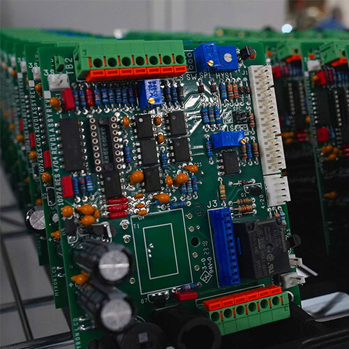
Circuit boards play a key role in making sure electronic products work properly. They provide structural support and link all the electrical parts together. Whether it’s in smartphones, laptops, or household devices, none could operate without a PCB. This guide will introduce you to the components of a printed circuit board and help you understand the manufacturing process.
Common Components of Printed Circuit Boards
Printed circuit boards are composed of various materials and electrical components. Here are some common PCB components:
Resistors
Resistors manage electrical current to create a specific voltage and convert excess electrical power into heat. They are available in various materials to suit different needs.
Capacitors
Capacitors store electrical energy and release it to power other parts of the circuit as needed. They operate by accumulating opposite charges on two conductive layers, separated by a non-conductive material.
Inductors
Similar to capacitors, inductors store energy but primarily block unwanted signals within the board to prevent interference from other electronic devices.
Transistors
Transistors amplify and manage electronic signals on the board. Among the different types, bipolar transistors are the most prevalent.
Transformers
These components transfer electrical energy between circuits by either increasing or decreasing the voltage.
Diodes
Diodes direct current to flow only one way, protecting the board and devices from electrical backflow. LEDs, or light-emitting diodes, are the most common type.
Sensors
These components identify shifts in the environment and translate those changes into corresponding electrical signals. These signals are then communicated to other components on the circuit board. Sensors transform physical phenomena like light, movement, air quality, or sound into electrical energy.
Layers of PCB
PCBs vary in complexity, but all share a foundational structure with four basic layers:
Substrate (FR4)
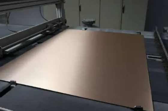
The substrate forms the base of the PCB, typically made from fiberglass, known as FR4. This material lends the board its robustness and ensures it maintains electrical insulation in various environments. FR4, short for “flame retardant,” combines woven fiberglass cloth with an epoxy resin binder to enhance fire resistance.
Copper Foil
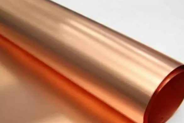
Above the substrate is a thin copper foil layer, adhered through heating. The number of layers on a PCB corresponds to how many layers of copper foil are present. PCBs range from single-sided with copper on one side to multi-layered versions with up to 100 layers, crafted by layering double-sided boards with insulating materials in between. This layering technique increases the wiring space within the board, essential for higher functionality.
Solder Mask
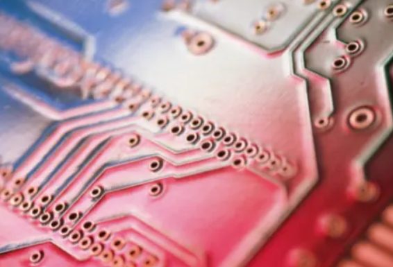
The solder mask sits atop the copper layer and gives PCBs their distinctive color, which varies but is often green. More than just aesthetic, the solder mask prevents electrical shorts by insulating the copper traces from direct contact with other metals, thereby safeguarding against circuit failures and soldering mishaps.
Silkscreen
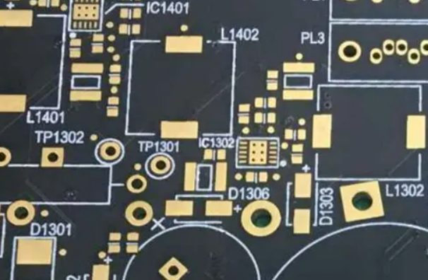
The final layer is the silkscreen, which applies directly to the solder mask. It provides crucial information, marking components, pins, and connections with symbols, letters, and numbers to simplify circuit board assembly and troubleshooting. Typically white for visibility, it may vary in color to contrast sharply with the solder mask, enhancing readability.
Steps in the Manufacturing Process of Printed Circuit Boards
Printed circuit boards, integral to electronic devices, comprise numerous parts that work in unison. Each board serves a unique purpose and function. Below are the main stages in the manufacturing process of circuit boards:
Designing the PCB
The journey of creating a printed circuit board kicks off with the design phase. Engineers and designers employ specialized software, like Extended Gerber (IX274X), to develop a detailed blueprint of the PCB’s layout and specifications. The variety in the shapes and forms of PCBs necessitates that their design must precisely match the intended device’s requirements, making the research and design phase very important.
Beyond design assistance, the software encodes fundamental data such as copper layer count, solder mask details, and component annotations. This information is indispensable before mass production commences.
Design Review and Engineering Considerations
Following the initial design, the PCB is scrutinized to ensure it meets specifications without errors. Engineers meticulously examine the design, searching for potential flaws or missing elements. Any overlooked errors can lead to costly consequences in later stages, including redesigns, prototyping, and testing. In severe cases, such mistakes can even jeopardize the entire product launch.
Once the design passes this review, it’s approved by the engineering team, and the process moves on to the printing phase.
Printing the PCB Design
The PCB design is printed on a specialized plotter printer, generating a film resembling a transparency. This film depicts the PCB layout. For inner layers, two ink colors are used: black for copper traces and clear for non-conductive areas. On outer layers, clear ink designates copper pathways, while black represents areas for copper removal. Registration holes are punched into the printed films to facilitate alignment in subsequent stages.
While advanced computer software and simulation are integral to the design process, the printed PCB design provides an additional opportunity for verification. Given the potential cost of errors, it’s essential to confirm proportions, wiring, and component placement before proceeding.
Creating the Printed Circuit Pattern
Next, the board’s conductive pattern is copper-plated. A positive photoresist material is applied to the foil surface, followed by a mask that’s exposed to ultraviolet light. This exposure renders the photoresist within the circuit design soluble. After removing the mask, you treat the board with an alkaline developer, revealing the underlying copper foil circuit design.
Chemical Etching of the Internal Layers
You then remove excess copper from the PCB’s inner layers. This is achieved through a chemical etching process that dissolves unwanted copper while preserving the necessary traces. The duration and intensity of this treatment depend on the specific design. This process requires a controlled environment to prevent damage to other PCB components. The goal is to ensure the conductor width adheres precisely to the blueprint.
Inner Layer Processing (For Multilayer PCBs only)
For multilayer PCBs, you next process the inner layers. This encompasses imaging, etching, resist stripping, post-etch punching, automated optical inspection, oxide application, layup, and lamination. These procedures ensure proper alignment, etching, and insulation for a functional multilayer board.
Align the Layers
Following this, you align the PCB layers using registration holes. An optical punch machine assists in this precise task. The interplay between outer and inner layers is very important, and even slight misalignments can compromise performance, durability, and functionality.
Automated Optical Inspection
This step uses automated optical Inspection (AOI) to identify defects. The AOI system compares the printed circuit boards to the Extended Gerber design, analyzing parameters such as circuit width and height, components, and connections. This automated inspection is essential for identifying and removing defective products on the assembly line, preventing errors from reaching the final product.
Laminating the PCB Layers
Here, layers are bonded using epoxy resin-soaked fiberglass and copper foil under high heat and pressure. This not only enhances the board’s structural integrity but also ensures continuous insulation between layers.
The Drilling Process
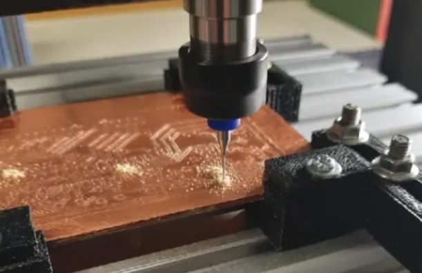
Once laminated, the PCB undergoes drilling, guided by X-ray to ensure accuracy. Registration holes are used, followed by deburring and the removal of excess copper. This drilling process is particularly important for multilayer PCBs, ensuring proper electrical connections between layers. Holes are drilled and deburred in a predetermined pattern, then lined with copper to create conductive pathways.
The PCB Plating Process
After cleaning the drilled PCB, you apply a thin layer of copper, just a few microns thick, to cover the uppermost layer and fill the drilled holes. This plating process protects the outer layers from moisture, contamination, and oxidation, while also improving aesthetics and solderability.
Outer Layer Imaging and Etching
You image the outer layer with photoresist and plate a protective layer of tin over the copper. The etching procedure removes unwanted copper and residual resist, leaving only the necessary copper design. Maintaining precise measurements is very important during this stage to ensure compatibility with the intended device.
PCB Surface Treatment and Finishing
Next, you apply a solder mask to the PCB. This mask prevents oxidation and erosion while also preventing conductivity between solder pads. The PCB is then cured at high temperatures in an oven. Following this, you print information such as the board’s serial number and origin onto its surface. A surface finish is then applied to prevent oxidation, with the specific finish chosen based on design specifications and the intended operating environment.
Final Quality Assurance and Delivery
Finally, you subject the PCB to a series of quality tests and inspections. The specific tests vary depending on the PCB type, but may include electrical reliability tests to evaluate circuit continuity and isolation. Profiling and routing methods isolate individual boards, while a CNC machine or router shapes and sizes them to the required specifications. A final check confirms hole sizes, dimensions, cleanliness, and overall quality.
Before shipping, you carefully package the PCBs to prevent damage during storage and transportation. Proper packaging is very important to protect the boards throughout the often complex and global supply chain
Free consultation with easy form that only takes 90 seconds
Feel free to contact us to ask about our products and services.


