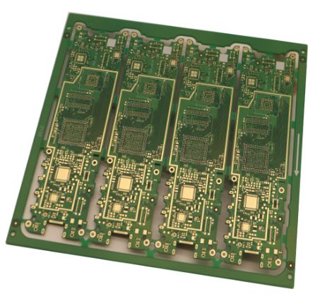
High-Speed PCB: Optimal Six-Layer Board Structure
When designing high-speed PCBs, the layer stack-up plays a crucial role in ensuring signal integrity, minimizing crosstalk, and achieving optimal electromagnetic compatibility (EMC). For a standard six-layer board with a thickness of 1.6mm, selecting the right structure can significantly impact performance. Below is an analysis of common six-layer board structures and their suitability for high-speed designs.
Standard Six-Layer Board Structure
A typical six-layer board consists of two core boards and two copper foils, laminated with PP glue (semi-cured film). This is widely used for conventional PCBs without high-speed signal requirements.
Structure Analysis
Structure 1: Top-GND-Signal_1-Signal_2-VCC-Bottom
- Features:
- Ground (GND) and Power (VCC) layers provide effective shielding.
- Top and Bottom layers are well-isolated from Signal_1 and Signal_2.
- Signal_1 and Signal_2 are separated by a distance of >20mil to reduce crosstalk.
- Pros:
- Excellent shielding between layers, reducing external interference.
- Suitable for designs with moderate signal routing density.
- Cons:
- Requires an eight-layer fabrication process (commonly referred to as a “fake eight-layer” board).
Structure 2: Top-Signal_1-GND-VCC-Signal_2-Bottom
- Features:
- Ground and Power layers are fully coupled, ensuring stable power delivery.
- Signal layers (Signal_1 and Signal_2) are closer to the Top and Bottom layers.
- Pros:
- Suitable for lower-frequency designs.
- Simple fabrication process.
- Cons:
- Higher potential for crosstalk due to insufficient isolation between Signal_1 and Signal_2.
- Limited shielding effectiveness.

Structure 3: Top-GND-Signal_1-VCC-GND-Bottom
- Features:
- Additional GND layer between Signal_1 and VCC improves shielding.
- Reduced number of signal layers (one fewer compared to other structures).
- Pros:
- Superior crosstalk prevention.
- Ideal for designs with high-speed signals requiring robust shielding.
- Cons:
- One fewer signal layer, potentially limiting routing space.
Selecting the Right Structure
The choice of stack-up depends on the circuit’s requirements, signal speed, and interference considerations:
- For high-speed signals:
- If routing can be managed on a single signal layer, Structure 3 is the best option due to its superior shielding capabilities.
- For moderate-speed signals or higher routing density:
- Structure 1 is the most balanced, offering effective shielding while accommodating multiple signal layers.
- For low-speed signals or cost-sensitive designs:
- Structure 2 is simpler and more cost-effective but less effective for high-speed applications.
Practical Example
The RK3399 embedded motherboard uses Structure 1, ensuring optimal performance with high-speed interfaces. Key specifications include:
- Impedance: Single-ended 50Ω, Differential 90Ω/100Ω.
- Crosstalk prevention: 40mil spacing between Signal_1 and Signal_2 layers.
This layout effectively isolates high-speed signals and minimizes crosstalk, making it ideal for embedded applications.
Key Considerations for High-Speed PCB Design
- Signal Integrity: Use proper spacing and shielding to maintain signal quality.
- Crosstalk Mitigation: Ensure adequate layer separation and avoid unnecessary vias.
- Power Integrity: Optimize GND and VCC coupling for stable operation.
- Impedance Matching: Follow design rules for controlled impedance routing.
By carefully selecting the layer structure based on circuit requirements, engineers can achieve reliable, high-performance PCB designs.


