High-Speed PCB Design Guide (Part 1): Basic Concepts of PCB
When designing high-speed PCBs, understanding the core concepts is crucial for ensuring efficiency and functionality. This guide introduces key elements such as layers, vias, pads, and more to help beginners and professionals alike.
1. The Concept of “Layer”
PCB layers represent the actual copper foil layers within the board material, unlike virtual layers in software. Modern electronic devices often use multilayer PCBs due to high component density and the need for robust anti-interference measures. Here’s what you need to know about layers:
- Types of Layers: PCBs can range from single-sided to multi-layered. For instance, a computer motherboard typically has more than four layers.
- Layer Functions: Internal layers often serve as power or ground planes (e.g., Ground and Power layers) and may use techniques like area filling for efficient routing.
- Vias and Layer Communication: Vias connect different layers, enabling signal or power transfer across the PCB.
- Design Tip: Disable unused layers to avoid confusion during design and manufacturing.
2. Understanding Vias
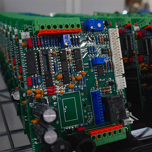
Vias are essential for interconnecting PCB layers. They are created by plating a conductive material inside drilled holes. Key points to consider:
- Minimize Via Usage: Use vias sparingly to reduce complexity and improve signal integrity.
- Size Matters: Larger vias handle higher currents, making them ideal for power and ground connections.
- Clearance: Ensure adequate spacing between vias and nearby traces to prevent short circuits.
3. Pads
Pads form the connection points for component leads on the PCB. While beginners may default to round pads, customizing them is crucial based on design requirements:
- Shape Selection: Consider round, square, octagonal, or custom shapes like teardrop pads for heat dissipation and mechanical strength.
- Pin Fit: Pad holes should be 0.2–0.4 mm larger than the component pin diameter.
- Asymmetric Pads: Useful for routing wires between pin angles.
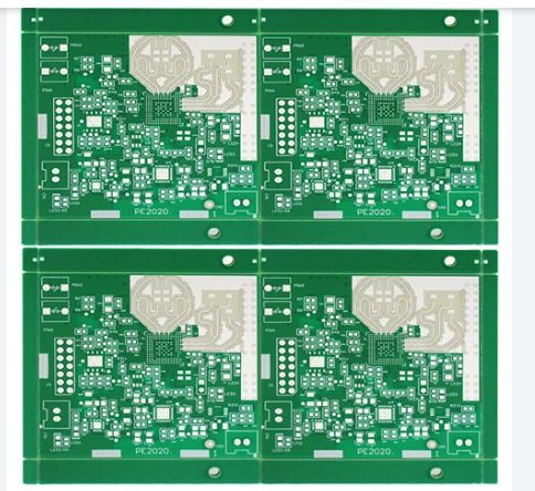
4. Silkscreen Layer (Overlay)
The silkscreen layer provides visual markers for assembly and maintenance. It includes text, symbols, and logos for component identification:
- Avoid Clutter: Ensure text doesn’t overlap with pads or solder areas.
- Readability: Place component numbers and other identifiers clearly to avoid ambiguity during assembly.
5. Surface-Mounted Devices (SMDs)
SMD components require special consideration due to their compact design and single-sided pin distribution:
- Correct Placement: Define the correct PCB side for SMDs to avoid missing pins.
- Text Labels: Ensure labels are placed on the same side as the SMDs.
6. Fill Areas: Grid-Shaped vs. Solid
When filling copper areas, choose between Grid-Shaped Filling Areas (External Plane) and Solid Filling Areas (Fill):
- Grid-Shaped Filling: Ideal for reducing high-frequency interference and creating shield areas or high-current paths.
- Solid Filling: Suited for small areas like line ends and corner regions.
7. Film Layers (Mask)
Mask layers are critical for soldering processes. They include:
- Solder Mask: Enhances pad solderability while preventing soldering on non-pad areas.
- Paste Mask: Complementary to the solder mask, it protects copper areas from unintended soldering.
8. Flying Wires (Fly Lines)
Flying wires have dual purposes in PCB design:
- Pre-Wiring Analysis: Simulate net connections to optimize component layout and improve automatic routing efficiency.
- Post-Routing Adjustments: Identify and manually connect unrouted nets using jumpers or 0-ohm resistors for production-ready designs.
Mastering the basics of PCB design—such as layers, vias, pads, and silkscreens—forms the foundation for creating high-speed, reliable boards. By understanding and applying these principles, designers can reduce errors and streamline both prototyping and manufacturing processes.

