High-Frequency PCB: High-Speed Circuits for Signal Transmission
PCB is the foundation used by electronics and electrical engineers in circuit design. It acts as a medium to connect components. Using PCB can eliminate the need for wires, make the circuit look less complicated, and make modifications easier. In layman’s terms, we can describe PCB as a laminate sandwich with additional components. It is designed with patchwork traces and planes that highlight the different components placed on it.
High-Frequency PCB is a subcategory in the field of PCB that is designed with extremely high electromagnetic frequencies. The typical frequency of high-frequency PCB is about 16 Ghz or higher. Since fast signal flow rate is required, the circuit design can be complex. Therefore, high transmission rate is required. With the advent of high-frequency PCB, this problem is a thing of the past. High-Frequency PCB is excellent in the signal requirements of integrating these electronic components.
What are the advantages of high-frequency PCB?
The following reasons highlight the advantages of high-frequency PCB when using PCB:
They are more efficient.
Efficiency improvement is a key advantage of high-frequency PCB. PCB with excellent efficiency is impressive because it can meet the heating needs of most devices. It also offers excellent environmental protection. The higher the efficiency, the more accurately the circuit can operate, and at the same capacity, the input power level can be even lower.
Higher Transmission Rate
For the vast majority of electrical devices, transmission speed is crucial. Thankfully, high transmission speed is also one of the advantages of high-frequency PCBs. It is very effective for signal transmission devices. Higher transmission speed allows data to be transmitted at a higher speed, allowing more data to be transmitted simultaneously.
High Temperature Control
High-frequency PCBs have excellent temperature control. Even at high temperatures, the PCBs perform at their best due to their excellent temperature control. This makes high-frequency PCBs ideal for high-temperature industries. Because of this, these PCBs are in high demand and are favored when manufacturing circuits that face high temperatures. The metal heating industry accounts for the majority of high-frequency PCB applications. Therefore, high-frequency PCBs are ideal for these industries because it offers high-temperature control.
High-frequency PCBs have high tolerances.
High-frequency PCBs have a sturdy structure that can withstand harsh weather. The materials used in their manufacturing absorb very little water and can withstand rainy days. In addition, it also has excellent peel strength, chemical resistance, and moisture resistance. It also provides additional protection for the circuit and its components in case of leakage of liquid or other liquid substances.
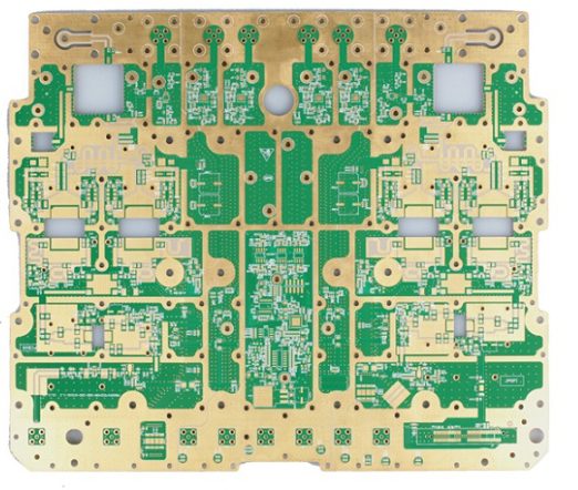
Features of High Frequency PCBs Make It Ideal for Signal Transmission
High frequency PCBs are widely used in the industry for signal transmission. Since PCBs have certain properties, they are ideal for signal transmission. High frequency PCBs have several characteristics. By understanding their characteristics, you will be able to understand these boards well. Due to these characteristics, they are called high frequency printed circuit boards. High frequency PCBs have several features, including:
Dissipation Factor
The low dissipation factor of high frequency PCBs is one of its most important characteristics. The dissipation factor of these PCBs ranges from 0.0019 to 0.025. This setting ensures that the signal transmission rate remains unchanged. It forms a small window for the propagation of data during transmission, allowing it to send data at a higher distance without causing energy pivoting. It will ensure that the data is not damaged during transmission. In addition, the common dissipation factor improves the signal transmission of the circuit. It helps reduce signal loss.
Stable and Lower Dielectric Constant
The dielectric constant of high frequency PCBs is lower and more stable, which is its important characteristic. This feature is crucial as it guarantees frequency transmission. Since the dielectric constant is low, this helps in reflection management and reduces the electrical length of the leads. It ensures significantly lower offset and charging delays. Also, it reduces signal lag. Moreover, lowering the dielectric constant enhances frequency transmission.
Chemical Resistant
High frequency PCBs can withstand chemicals. They are designed to be excellent when exposed to chemical attack. Hence, there is a lower risk of these boards getting rusted. Since high frequency PCBs are highly resistant to most of the corrosive chemicals, they are very useful when making circuits in close proximity to chemicals and leaky batteries. This is also one of the main reasons why the PCBs used in chemical projects are mostly high frequency PCBs.
Resistant to Humid Environments
These PCBs are manufactured with minimum water absorption in mind. The materials selected ensure that there is little to no water absorption. Since the board cannot absorb moisture or other substances, it can easily withstand humid environments. This makes high frequency PCBs invaluable in circuit designs that are intended to be used in humid environments. These PCBs are even tested to be best suited for rainy days and are often used in such environments to ensure that they perform to their full potential. It is essential for circuits in remote areas with high rainfall and similar conditions.
Low Dimensional Stability
The low dimensional property is another essential characteristic of high frequency PCBs. They can maintain their size and shape regardless of temperature. There is no difference in their dimensions whether they are exposed to hot or cold areas. Since these PCBs do not deform at different temperatures, these PCBs are essential and irreplaceable in extreme temperature scale environments. This characteristic sets them apart and makes them compatible with conditions and regions in remote areas of the globe. They perform well and since they are highly tolerant to the weather conditions they are exposed to, you do not need to check them often for maintenance which would be disastrous for other PCBs.
Additional Guidelines When Designing or Using High Frequency PCBs in Your Circuits
When designing or using high frequency PCBs, it is important to keep in mind critical details. Due to their unique characteristics, these PCBs must be handled with extra care and require a higher degree of caution and care. Here are some guidelines that are recommended for you to follow before working with high frequency PCBs:
Focus on Your Design
Before you start your PCB design, it is essential to have a plan in advance. By doing this, you can avoid anything that could harm your design. An important strategy to achieve this goal is to create a checklist. Before you sit down to implement the PCB, make sure to work out the details on paper as they are sensitive and need to be handled with care.
Determine the signal frequency of the PCB
Make sure to verify the voltage and power requirements of the integrated circuits. Determine the division of any power planes. Also, you need to confirm the adaptability of the various signals. The manufacturer helps to ensure the lowest tolerance standards. It would help if you have a strategy to reduce the noise level of high-frequency communications. It is essential to ensure that your PCB works efficiently. As the name suggests, frequency establishment is key to this PCB, and handling it is essential to make the most of high-frequency PCBs.
Understand the limitations of the circuit to create the perfect environment for the PCB
Writing down the requirements of the stacked layers is essential when you start thinking about how to design the PCB. You can ask the manufacturer to assist in sourcing the precise materials for the PCB. You must understand the specific limitations and components of the printed circuit board. Not adapting to the constraints of the materials used in the PCB design can lead to unforeseen disasters when running/testing the circuit. The best way to ensure that the circuits perform to their maximum potential is to ensure that they are provided with ideal working conditions.
Setting Power and Ground Planes
After defining the PCB layout, it is imperative to check the design. The reason is that you should understand the ground plane. Using routing signals to separate the ground plane may not be necessary. If you divide the ground plane, you should also rotate the gap. Signal timing and EMI may be affected by this. The ground plane must be separated. Be careful to include a resistor in the signal trace. The signal will have a gap, which improves the return path.
Route Frequency Signals
You can route frequency signals to take advantage of the additional shielding capabilities of this board. High frequency signals emit a lot of radiation. It can cause interference between two different transmissions. You can prevent this from happening by routing frequency signals. Create an excellent current return path because every signal on a high frequency PCB needs a path. The path starts from the source and leads all the way to the receiver. Just block that path. It plays a vital role in the creation of RF substrates.
High frequency PCB is a critical part of the PCB world. It is an essential part of communication technology, both now and in future advancements. Understanding how high frequency PCB works and how important it is to the world can help change your perspective on the importance of PCBs. They add completely different properties to your circuit, rather than just being a placeholder for wires, they provide a foundation for components to build on. High frequency PCBs are essential to imparting their properties to your circuit and improving it.

