


High-Frequency PCB Assembly Case Study: High-Precision Communication Equipment
Customer Background: Our customer is a leading communication equipment company specializing in the development and manufacturing of high-frequency devices for 5G communication systems. Due to the high-frequency signal transmission requirements of their products, their PCB design demands extremely high signal integrity and strong anti-interference capabilities.
Product Complexity: The primary challenge of this project was ensuring that the high-frequency PCB maintained extremely low attenuation and distortion during signal transmission while preventing external interference from affecting signal quality. To achieve this, the PCB required specialized materials and layout design, along with precise signal connections and low-impedance matching during the assembly process.
Key Technical Challenges in the Assembly Process
- Material Selection: As the device operates at frequencies above 6GHz, traditional FR4 materials were insufficient. We selected RO4350B and Teflon high-frequency materials, which feature low dielectric constants and excellent signal transmission properties, making them ideal for high-frequency circuit design.
- Precision Signal Line Design: To ensure signal integrity, we implemented microstrip and stripline structures. In high-frequency PCBs, every detail of the signal path must be precisely calculated to prevent unnecessary reflections and interference.
- Low-Impedance Matching: One of the core requirements of high-frequency PCBs is impedance matching. We strictly controlled the impedance of each signal line to maintain consistency and prevent signal reflection-induced interference. High-precision impedance measurement instruments were used to ensure that every signal layer’s impedance remained within the design specifications.
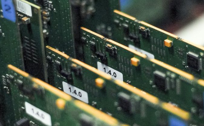
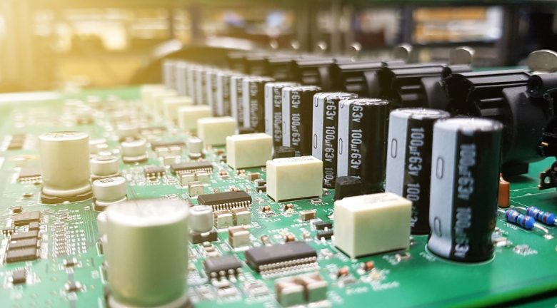
- High-Precision SMD Component Assembly: High-frequency circuits impose strict requirements on component size, layout, and spacing. All surface-mount components (such as high-frequency inductors, capacitors, and transistors) were assembled using advanced SMT (Surface Mount Technology). During the soldering process, we used lead-free solder and precisely controlled soldering temperature and duration to prevent any impact on the electrical performance of the components.
- Soldering and Testing: In high-frequency PCB assembly, we paid particular attention to soldering quality, using precision reflow soldering equipment and conducting rigorous solder joint inspections. Each solder joint was X-ray inspected to ensure there were no cold joints or cracks. After assembly, each PCB underwent comprehensive signal integrity testing and high-frequency testing to ensure the product met the required performance standards in real-world applications.
6. EMI (Electromagnetic Interference) and Shielding: High-frequency signals are highly susceptible to electromagnetic interference. To address this, we incorporated dedicated shielding layers into the PCB design and used metal enclosures for additional protection. Additionally, the PCB surface was gold-plated to reduce surface losses and enhance signal transmission efficiency.