


high-frequency PCB
What is high-frequency PCB?
High-frequency PCB board or RF microwave PCB refers to the special circuit board with high electromagnetic frequency, which is used for high frequency (frequency greater than 300MHz or wavelength less than 1m). Generally speaking, a high-frequency board can be defined as a circuit board with a frequency above 1GHz. Substrate materials need to have excellent electrical properties and good chemical stability. With the increase of power signal frequency, the loss requirement on the substrate is very small, so the importance of high-frequency material is highlighted.
High-frequency PCB board with induction heating technology has been widely used in the communication industry, network technology, and high-speed information processing system, which meets the requirements of many high-precision parameter instruments. A reliable high-frequency circuit board, in the actual production, provides great help.
High-frequency PCB is widely used in RF and Microwave PCB. High-frequency PCB materials are different from conventional FR4 materials. Most of them use PTFE &Teflon materials. Good electrical properties and low signal loss are the basis.
High-frequency PCB needs special materials to realize the high-frequency signal provided by this type of printed circuit board. Many PCB designers choose Rogers dielectric material because of its lower dielectric and signal loss, lower circuit manufacturing cost, and more suitable for rapid turnover prototype application.
In addition to selecting the right PCB material and determining the correct Er value, the designer should also consider the conductor width and spacing, substrate constant, and other parameters. The highest level of process control must be used to specify and implement these parameters precisely.
KKPCB is an experienced full-service high-frequency PCB manufacturer, which can provide reliable and excellent high-frequency PCB fabrication services. Evaluate your requirements according to your design, rich variety of high-frequency materials, mature high-frequency PCB manufacturing experience.
KKPCB is an experienced full-service high-frequency PCB manufacturer, which can provide reliable and excellent high-frequency PCB fabrication services. Evaluate your requirements according to your design, mature high-frequency PCB manufacturing experience. Professional production experience for high frequency circuit boards used in power divider, coupling and device, circuit builder, amplifier, dry release, base station 3G antenna. Company year-round stocks domestic and imported high-frequency material (F4B Rogers, TACO, NC, ARLON, TP-2) dielectric constant 22106, etc. Can provide fast sample service and mass production in time to meet your diverse, multi-variety needs.
What are the advantages of high-frequency PCB?
High efficiency
A High-frequency circuit board with a small dielectric constant will also have a small loss, and the advanced induction heating technology can meet the demand of target heating, and the efficiency is very high. Of course, while focusing on efficiency, it also has the characteristics of environmental protection, which is very suitable for the development direction of today’s society.
Fast
The transmission speed is inversely proportional to the square root of the dielectric constant, which means that the smaller the dielectric constant, the faster the transmission speed. This is the advantage of high-frequency PCB, it uses special material, not only to ensure the characteristics of small dielectric constant but also to maintain stable operation, which is very important for signal transmission.
A large degree of regulation
High-frequency circuit boards, which are widely used in various industries for the heating treatment of precision metal materials, can not only realize the heating of components with different depths but also focus on heating according to the local characteristics. Whether the heating methods of surface or deep level, concentration or dispersion can be easily completed.
It is well tolerated
The dielectric constant and medium have certain requirements on the environment. The use of the circuit board will be seriously affected by humid weather. The high-frequency circuit board made of materials with low water absorption can challenge this environment. At the same time, it has the advantages of resistance to chemical corrosion, moisture resistance, high-temperature resistance, and great peel strength, which makes the high-frequency circuit board play a strong performance.
Processing characteristics of high-frequency PCB
Impedance control requirements are relatively strict, relative to the line width control is very strict, with the general tolerance of about 5-8%.
Due to the special material, so the adhesion of PTH copper is not high. It is usually necessary to roughen the via hole and surface with the help of plasma treatment equipment to increase the adhesion of PTH hole copper and solder mask ink.
Do not grind the board before the solder mask, otherwise, the adhesion will be very poor, only use a micro etching solution to roughen.
Most of the materials are made of polytetrafluoroethylene, and there will be a lot of burrs formed by ordinary milling cutters, so a special milling cutter is needed.
Its physical properties, precision, technical parameters requirements are very high, commonly used in automotive anti-collision systems, satellite systems, radio systems, and other fields.
Application field of high-frequency PCB
Mobile communication products, intelligent lighting system
Power amplifier, low noise amplifier, etc
Power divider, coupler, duplexer, filter, and other passive components
In the fields of automobile anti-collision systems, satellite systems, and radio systems, the high frequency of electronic equipment is the development trend.
Classification of high-frequency PCB material
Powder ceramic filled thermosetting materials
A. Manufacturer: Rogers 4350b / 4003c, Arlon 25N / 25FR, Taconic TLG series
B. Processing method:
The processing process is similar to that of epoxy resin/glass woven fabric (FR4), but the board is brittle and easy to break. When drilling and punching, the service life of the drill bit and Gong knife will be reduced by 20%.
PTFE material
A: Manufacturer
1. Rogers Ro3000 series, RT series, and TMM series
2. Arlon AD / AR series, isoclad series, and cuclad series
3. Taconic RF series, TLX series, and TLY series
4. F4B, F4BM, F4BK, TP-2 of Taixing microwave
B: Processing method
1. Cutting: the protective film must be reserved to prevent scratch and indentation
2. Drilling:
Use a new drill bit (standard 130, presser foot pressure is 40psi
The aluminum sheet is the cover board, and then use 1 mm melamine backing board to tighten the PTFE board
After drilling, blow out the dust in the hole with an air gun
With the most stable drilling rig, the drilling parameters (basically, the smaller the hole, the faster the drilling speed; the smaller the chip load, the smaller the return speed)
3. Hole treatment
Plasma treatment or sodium activation treatment is beneficial to pore metallization
4. PTH copper deposition
After micro etching (the micro erosion rate is controlled by 20 micro inches), the board is fed from the oil cylinder after PTH pulling
If necessary, the second PTH will be passed, and the board can only be fed from the predicted cylinder
5. Soldermask
Pretreatment: acid washing, not mechanical grinding
After pretreatment, bake the board (90 ℃, 30min), brush green oil to solidify
Three stages of baking: 80 ℃, 100 ℃ and 150 ℃ for 30min respectively (if oil is found on the surface of the substrate, rework can be done: wash off the green oil and reactivate it)
6. Gong board
Lay the white paper on the surface of the PTFE board line, and clamp it with FR-4 baseboard or phenolic baseboard with a thickness of 1.0 mm to remove copper:
The rough edge of the backboard of the Gong board needs to be carefully scraped by hand to prevent damage to the base material and copper surface, and then separated with sulfur-free paper of a certain size, and visual inspection should be carried out to reduce the burr. The key point is that the removal effect of the Gong board process should be good.
List of common high speed and high-frequency PCB material parameters
List of common high speed and high-frequency PCB material parameters | ||||||||||||
supplier | board | Resin type | Material properties | price index | application area | Evaluation conclusion | ||||||
DK | DF | Tg | Td | Z-CTE | T288 | Water absorption | ||||||
(1GHZ) | (1GHZ) | (DSC) | (TGA) | (50-260) | (min) | (%) | ||||||
SYST | S7439(EL230T) | / | 3.8 | 0.0045 | 200℃ | 380℃ | / | >60min | 0.08% | / | Network equipment, measuring equipment | |
S7240 | / | 3.9 | 0.005 | 200℃ | 360℃ | 2.00% | >60min | 0.10% | / | Backplane, server, router | ||
EL190T | / | 4.3 | 0.011 | 220℃ | 345℃ | / | 20min | / | / | / | ||
FL700 | / | 3.7 | 0.003 | 205℃ | 350℃ | / | 20min | / | / | / | ||
FL700LD | / | 3.5 | 0.0025 | 205℃ | 350℃ | / | 20min | 0.24% | / | / | ||
ITEQ | IT200LK | / | 3.8 | 0.01 | 200℃ | 350℃ | 2.50% | 30min | 0.10% | / | / | |
IT150DA | / | 3.56 | 0.0047 | 172℃ | 350℃ | 3.81% | 30min | 0.12% | / | / | ||
ISOLA | FR408 | FR4 + hydrocarbons | 3.77 | 0.011 | 180℃ | 360℃ | 3.50% | 20 | 0.15% | / | / | Board thickness ≤ 2.0mm, pitch ≥ 0.8mm |
FR408HR | 3.68 | 0.009 | 200℃ | 370℃ | 2.80% | 30 | 0.06% | 3.2 | / | Board thickness ≤ 3.0mm, pitch ≥ 0.8mm | ||
IS680-345 | / | 3.45 | 0.0035 | 192℃ | 376℃ | 2.90% | 60min | 0.10% | 5 | / | ||
NECLO | N4103-13 | CE (cyanate ester) | 3.7 | 0.009 | 210℃ | 365℃ | 3.40% | 10 | 0.10% | 3.9 | Automotive, aviation, defense, communications infrastructure, semiconductors, high-speed data | |
N4103-13EP | 3.7 | 0.009 | 210℃ | 350℃ | 3.50% | 10+ | 0.10% | 3.9 | ||||
N4103-13SI | 3.4 | 0.008 | 210℃ | 365℃ | 3.50% | 10+ | 0.10% | 3.9 | ||||
N4103-13EPSI | 3.4 | 0.008 | 210℃ | 350℃ | 3.20% | 10+ | 0.10% | 4.3 | ||||
Mercurywave 9350 | / | 3.7 | 0.004 | 200℃ | 360℃ | 2.50% | 40min | 0.15% | / | |||
Panasonic | M4 (R5725) | FR4+PPO | 3.8 | 0.005 | 175℃ | 362℃ | 2.80% | 30 | 0.14% | 4 | ||
M6 (R5775K) | PPO | 3.6 | 0.002 | 185℃ | 410℃ | / | 60min | 0.14% | 5.8 | |||
TUC | TU-872/SLK | / | 3.8 | 0.008 | 200℃ | 340℃ | / | 20min | / | 3.3 | / | |
TU-872/SLKSP | / | / | / | / | / | / | / | / | /3.3 | / | ||
EMC | EM828 | / | 3.7 | 0.008 | 170℃ | 380℃ | / | 30min | / | / | / | |
HITACHI | FX-2 | / | 3.5 | 0.002 | 180℃ | 350℃ | / | 60min | 0.03% | 10.3 | / | |
MCL-LX-67 | / | 3.5 | 0.005 | 235℃ | / | / | / | 0.03% | 8.4 | / | ||
ROGERS | RO4350B | Hydrocarbons + ceramics | 3.48 | 0.0031 | 280℃ | 390℃ | 0.63% | 60min | 0.06% | 8.3 | Satellite TV LNB, microstrip line, power amplifier | |
RO3003 | PTFE ceramics | 3 | 0.0013 | / | 500℃ | / | / | <0.1% | 16.7 | Communication satellite, backplane | ||
RO4533 | PTFE ceramics | 3.3 | 0.0025 | / | 500℃ | / | / | <0.02% | 25 | Cellular base station antenna | ||
RO3730 | PTFE ceramics | 3 | 0.0016 | / | 500℃ | / | / | 0.04% | 25 | Base station antenna, the satellite transmission antenna | ||
ARLON | TC350 | PTFE ceramics | 3.5 | 0.002 | / | 567℃ | 1.20% | >60min | 0.05% | 6.5 | Power amplifier, filter, connector | |
AD300C | PTFE ceramics | 2.97 | 0.002 | / | 555℃ | / | >60min | 0.06% | 8.3 | Base station antenna, power amplifier | ||
CLTE-AT | PTFE ceramics | 3 | 0.0013 | / | 529℃ | / | >60min | 0.03% | 16.5 | Car radar, sensor | ||
Multiclad | / | 3.7 | 0.004 | 205℃ | 432℃ | 1.20% | >60min | 0.10% | 4 | Backplane, power amplifier, receiver | ||
TACONIC | RF35A2 | PTFE + glass fiber | 3.5 | 0.0011 | / | 528℃ | 2.65% | / | 0.02% | 18 | Wireless link, transmitter, power divider, combiner, filter, base station antenna | |
TLY-5 | PTFE + glass fiber | 2.2 | 0.0009 | / | / | / | / | <0.02% | / | |||
TSM-30 | PTFE + glass fiber | 3 | 0.0015 | / | / | / | / | 0.03% | 36 | |||
TLX-8 | PTFE + glass fiber | 2.45 | 0.0015 | / | / | / | / | <0.02% | / | |||
RF35 | PTFE + glass fiber | 3.5 | 0.0018 | / | / | / | / | 0.03% | 14 | |||
TLC-30 | PTFE + glass fiber | 3 | 0.028 | / | / | / | / | <0.02% | / | |||
High-frequency PCB manufacturing flow
1. Npth PTFE board processing process
Cutting – Drilling – dry film – Inspection – etching – etching checking – solder mask- character – HASL– forming – testing – final inspection – Packaging – Shipping
2. PTFE board processing flow of PTH
Cutting – Drilling – Plasma treatment or sodium naphthalene activation treatment-PTH- Plate plating – dry film-Inspection- pattern plating-etch-inspection-solder mask-silkscreen-HASL-profiling-test-FQC-packaging-shipping
Difficulties in high-frequency board processing
1. Copper deposition: the hole wall is not easy to deposit copper
2. Control of line gap and sand hole in graph rotation, etching, and line width
3. Green oil process: green oil adhesion, green oil foaming control
4. The scratch on the board surface is strictly controlled in each process
The advantage of Rogers PCB materials prototyping and costs
1. The commonly used high-speed boards are as follows:
TUC: Tuc862, 872slk, 883, 933, etc.
Panasonic: megtron4, megtron6, etc. ,
Isola: fr408hr, is620, is680,
Nelco: n4000-13, n4000-13epsi,
Dongguan Shengyi, Taizhou Wangling, Taixing microwave, etc
Rogers circuit board is very popular in the market. Rogers brand materials are mostly used in the high-frequency communication industry.
2. Main substrate of Rogers circuit board
Rogers 4350b is one of the boards imported from Rogers, USA, which is mainly used in the production of high-frequency circuit boards. In addition, there are also ro4350b, ro4003c, rt5880, ro3003, and ro3010. For detailed parameters, please refer to the materials data sheet on Rogers’s website.
Rogers high-frequency board is usually mixed with special materials
Rogers and special materials, copper-based materials + Rogers become Rogers hybrid copper substrate PCB, and ceramic base + FR4 are Rogers communication hybrid base board, etc,
3. The cost of Rogers circuit board prototyping
Rogers high-frequency board prototyping costs note that there are a few aspects of the composition,
Rogers base material model
The process requirement, the more complex the process, the more expensive the price
The number of layers, the higher the number of layers, the price will increase accordingly, and the difficulty of making boards will also increase
In addition, there are engineering costs. If there is an urgent need, there are also urgent costs, etc
High-frequency PCB manufacturing in KKPCB
KKPCB is a professional high-frequency PCB board manufacturer. Rogers high-frequency PCB prototyping is more done in the high-frequency board. In addition, there are other high-frequency materials, such as tekonik high-frequency board, PTFE high-frequency board, Arlon, etc.
KKPCB has 20 years of PCB production experience, 300 skilled technical teams, professional PCB and PCBA quality inspection team, to ensure product quality, delivery on time, high-frequency board as soon as 48 hours delivery, 24 hours uninterrupted quotation, timely solve customer problems. Please consult KKPCB for more details.
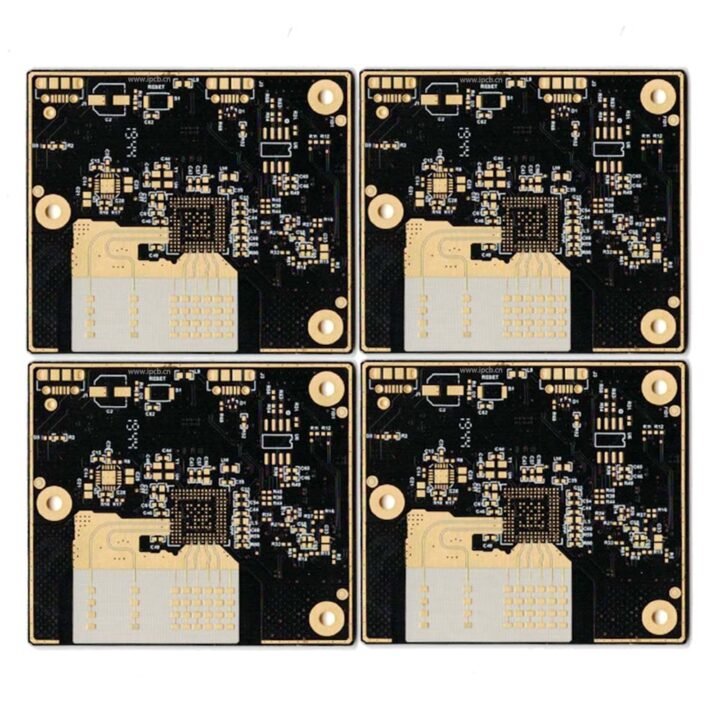
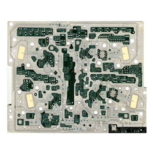
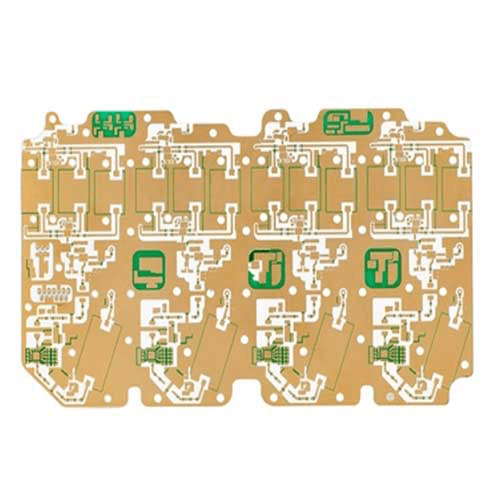
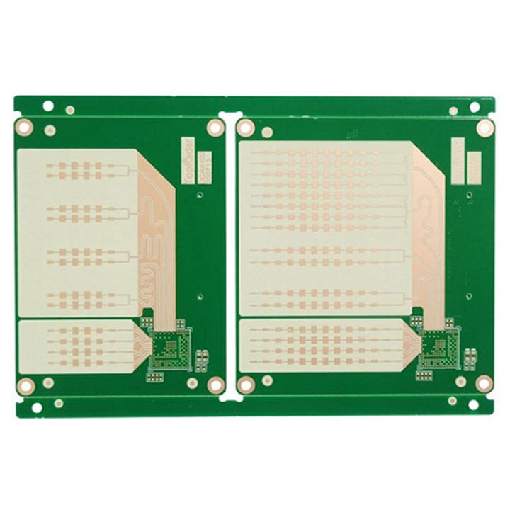
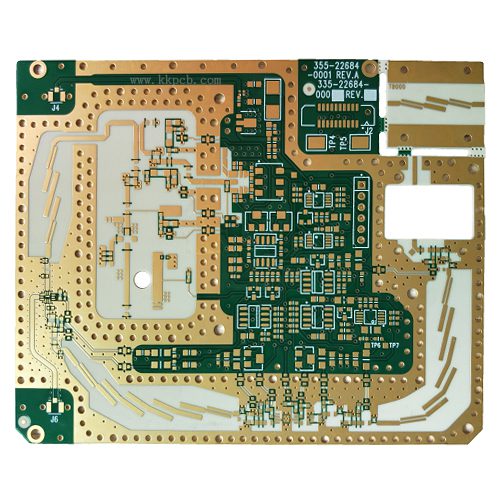
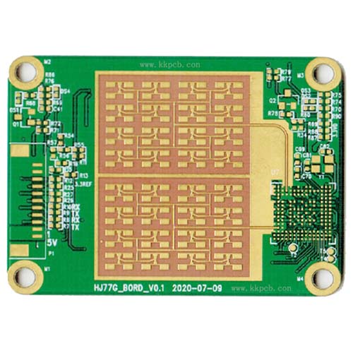
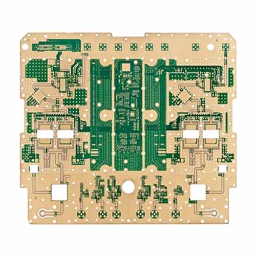
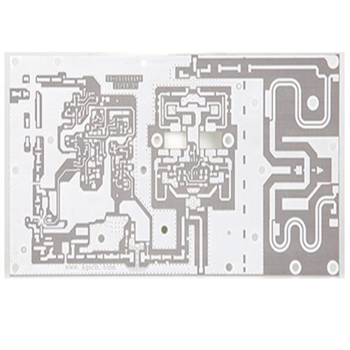
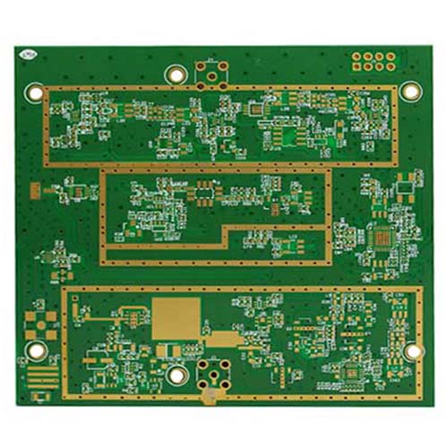
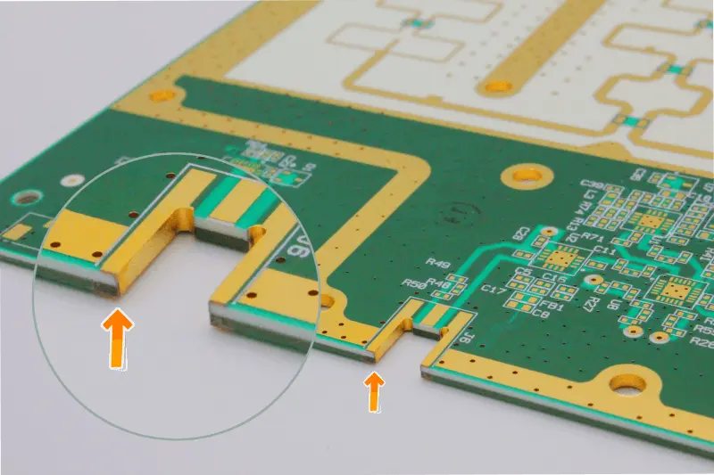
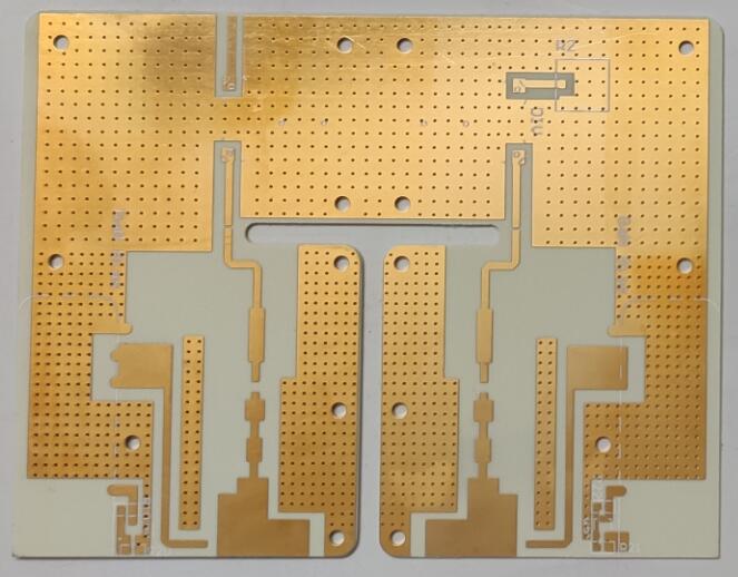
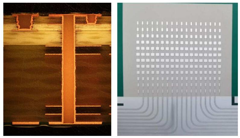
Actual Product Cases
| Basic product information | 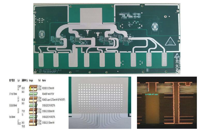 | |||||||||
| Number of layers | 8L | |||||||||
| The thickness of the finished board | 2.0±0.2mm | |||||||||
| Finished product size | 11.81×6.44inch | |||||||||
| Aspect ratio | Through hole 7:1, blind hole 0.63:1 | |||||||||
| Board material | RO3003+RO4835LowPRo + s1000-2 hybrid | |||||||||
| Minimum drill tip/Finished hole size | 0.275/0.2mm | |||||||||
| Minimum line width/Line spacing | 0.102/0.114mm | |||||||||
| Back drill | Stub control 8mil | |||||||||
| Impedance tolerance | ±10% | |||||||||
| surface treatment | Immersion Silver | |||||||||
| HDI design; Back drilling; Mixed compression of three materials; Impedance control; Pofv process; 77GHzRadio frequency microwave radar | ||||||||||
| Basic product information |
| |||||||||
| Number of layers | 8L | |||||||||
| The thickness of finished board | 2.0±0.2mm | |||||||||
| Finished product size | 11.81×6.44inch | |||||||||
| Aspect ratio | Through-hole 7:1, blind hole 0.63:1 | |||||||||
| Board material | MT-77+RO4835LowPro+S1000-2 mixed pressure | |||||||||
| Minimum drill tip/Finished hole size | 0.275/0.2mm | |||||||||
| Minimum line width/Line spacing | 0.102/0.114mm | |||||||||
| Back drill | Stub control 8mil | |||||||||
| Impedance tolerance | ±10% | |||||||||
| Surface treatment | Immersion Silver | |||||||||
| HDI (L1-L3 macroporous laser); Back drilling; Mixed compression of three materials; Impedance control; Pofv process 77GHz RF microwave radar | ||||||||||
| Basic product information | 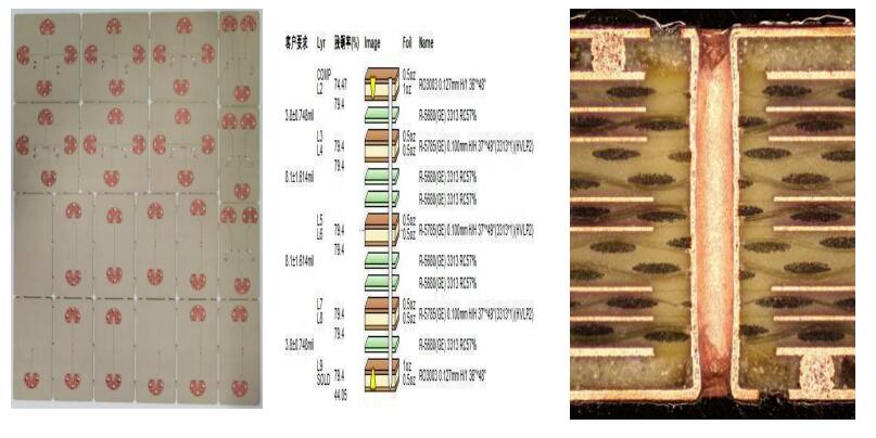 | |||||||||
| Number of layers | 10L | |||||||||
| The thickness of finished board | 1.4±0.14mm | |||||||||
| Finished product size | 15.66×12.24inch | |||||||||
| Aspect ratio | Through-hole 5.4:1, blind hole 0.93:1 | |||||||||
| Board material | Ro3003 + r5785 mixed pressure | |||||||||
| Minimum drill tip/Finished hole size | 0.25/0.2mm | |||||||||
| Minimum line width/Line spacing | 0.13/0.1mm | |||||||||
| Back drill | N/A | |||||||||
| Impedance tolerance | ±10% | |||||||||
| surface treatment | OSP | |||||||||
Large size panel design; HDI; Microwave RF board; High frequency mixed pressure, electroplating hole filling; steam Car board (77GHz RF microwave radar ) | ||||||||||
| Basic product information | 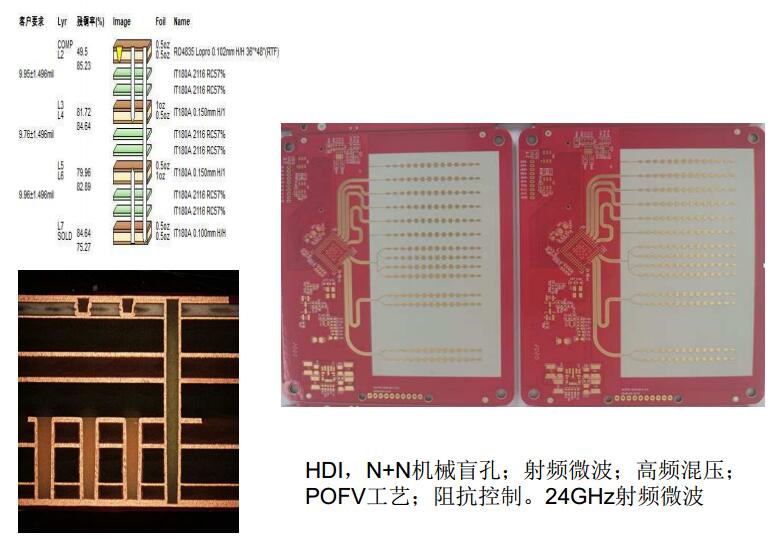 | |||||||||
| Number of layers | 8L | |||||||||
| The thickness of finished board | 1.6±0.16mm | |||||||||
| Finished product size | 5.98*3.94 | |||||||||
| Aspect ratio | Through-hole 6:1, blind hole 0.58:1 | |||||||||
| Board material | Mixed pressure of ro4835 + it180a(n + n structure) | |||||||||
| Minimum drill tip/Finished hole size | 0.25/0.2mm | |||||||||
| Minimum line width/Line spacing | 0.102/0.114mm | |||||||||
| Back drill | N/A | |||||||||
| Impedance tolerance | ±10% | |||||||||
| surface treatment | Immersion Nickel gold | |||||||||
| HDI, N + n mechanical blind hole; Radio frequency microwave; High frequency mixed pressure; Pofv process; Impedance control.24GHz RF microwave | ||||||||||
| Basic product information | 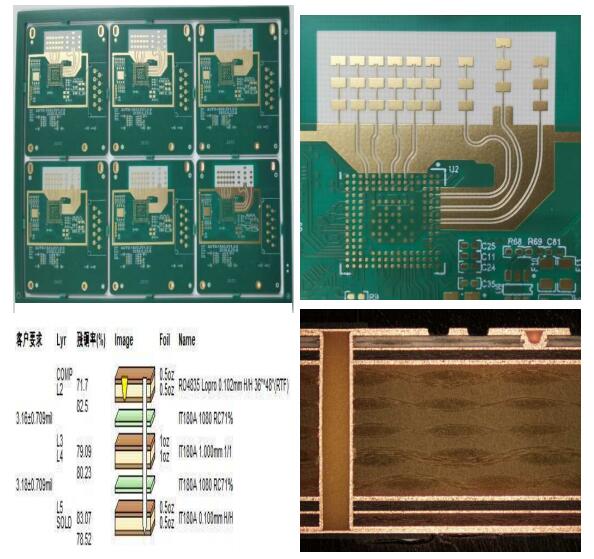 | |||||||||
| Number of layers | 6L | |||||||||
| The thickness of finished board | 1.6±0.16mm | |||||||||
| Finished product size | 6.79×5.08inch | |||||||||
| Aspect ratio | Through-hole 5.9:1, blind hole 0.58:1 | |||||||||
| Board material | RO4835+IT180A | |||||||||
| Minimum drill tip/Finished hole size | 0.25/0.2mm | |||||||||
| Minimum line width/Line spacing | 0.102/0.114mm | |||||||||
| Back drill | N/A | |||||||||
| Impedance tolerance | ±10% | |||||||||
| surface treatment | Immersion Nickel gold | |||||||||
HDI; POFV; impedance; Mixed pressure; 24GHz radio; Frequency microwave | ||||||||||
| Basic product information | 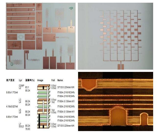 | |||||||||
| Number of layers | 8L | |||||||||
| Thickness of finished board | 1.64±0.17mm | |||||||||
| Finished product size | 13.78*12.81 | |||||||||
| Aspect ratio | Through hole 6.1:1, mechanical blind hole 1.17:1 | |||||||||
| Board material | S7135 + it180a mixed pressure | |||||||||
| Minimum drill tip/Finished hole size | 0.25/0.2mm | |||||||||
| Minimum line width/Line spacing | 0.5/0.127mm | |||||||||
| Back drill | Three kinds of mechanical PTH depth control drilling | |||||||||
| Impedance tolerance | N/A | |||||||||
| surface treatment | Immersion Silver | |||||||||
| Large panel; Mechanical blind hole plate; Microwave radio frequency; Mixed pressure, different depth back drilling | ||||||||||
| Basic product information | 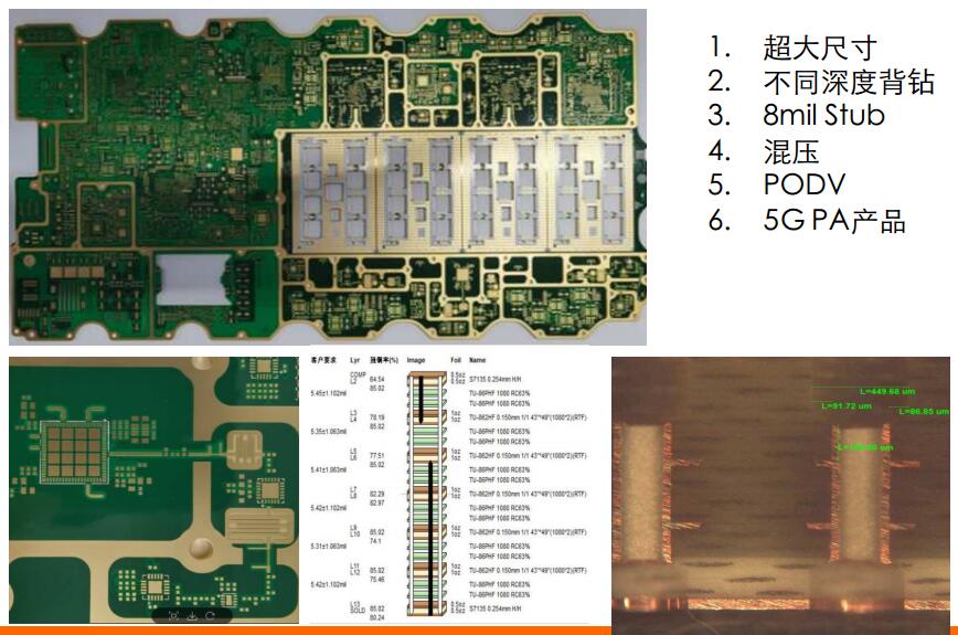 | |||||||||
| Number of layers | 14L | |||||||||
| Thickness of finished board | 2.5±0.25mm | |||||||||
| Finished product size | 21.73*10.91inch | |||||||||
| Aspect ratio | 9.8:1 | |||||||||
| Board material | TU-862HF+S7135 | |||||||||
| Minimum drill tip/Finished hole size | 0.25/0.2mm | |||||||||
| Minimum line width/Line spacing | 0.114/0.114mm | |||||||||
| Back drill | Double side back drilling, stub value in the same hole control 8 mil | |||||||||
| Impedance tolerance | ±10% | |||||||||
| surface treatment | Immersion Nickel gold | |||||||||
| Oversize; Different depth back drilling; 8mil Stub; Mixed pressure; PODV; 5G PA product | ||||||||||


