HDI Printed Circuit Board (PCB)
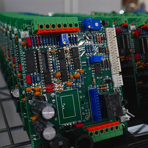
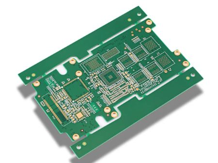
What’s HDI PCB? High-density interconnect (HDI) PCBs are characterized by finer lines, closer spaces, and more dense wiring, which allow for a faster connection while reducing the size and bulk of a project. These boards also feature blind and buried vias, laser ablated microvias, sequential lamination, and via in-pads.
As a result, a HDI board can house the functionality of the previous boards used. KKPCB is an HDI PCB manufacturer and provider in Shenzhen, China supports HDI PCB prototype and mass production with less expensive price and quick-turn lead time. Customers from a variety of industries we serve have a common that have high expectations in quality, reliability and on-time delivery in HDI PCB production. Our quality is not afterthought, but built into each process from front-end to fabrication and shipping.
HDI PCB Manufacturing Process
The overall process for manufacturing HDI PCB is essentially the same as for fabricating other PCB board, with notable differences for PCB stack-up and hole drilling. Since HDI boards generally require smaller drill holes for vias, laser drilling is usually required. Although laser drills can produce smaller and more precise holes, they are limited by depth. Therefore, a limited number of layers can be drilled through at a time. For HDI boards, which are invariably multilayer and may contain buried and blind vias, multiple drilling processes may be required. This necessitates successive layer boding to achieve the desired stack-up or sequential lamination cycles. Not surprisingly, this can significantly increase PCB manufacturing time and cost.
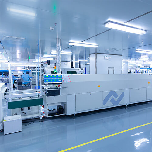
HDI PCB fabrication is an advanced technology and therefore requires expertise along with specialized equipment like laser drills, laser direct imaging (LDI) capability, and special clean room environments. In order to efficiently manufacture high-quality and reliable HDI PCB products, you must understand the HDI board manufacturing process and coordinate with your HDI PCB supplier to implement good DFM (Design for Manufacturability) for HDI layout design.
Click to check our PCB Fabrication Process and PCB Capabilities
HDI PCB Design
The electronics industry is largely consumer-driven and the directive for smaller more capable products with increased functionality will only intensify in the years to come. At KKPCB, we are well-positioned to assist you in meeting this demand with advanced equipment, processes and expertise to manufacture your HDI PCB boards quickly and precisely.
HDI, with its attendant reduction in size and weight, goes hand in hand with this greater density of surface mount components. Of course, the high count connections for integrated circuits and components including BGAs and flip chips simply adds to the need for HDI. Because of fine lines and blind microvias design, the dimple and bump after via filling are the two parameters to check whether the HDI printed boards reach your thin copper deposited requirement. HDI layout always refer to DDR3, DDR4, XAUI, PCIe, LVDs, Gig-E applications, the designs always include high-speed stripline and microstrip, your PCB fabricator should have advanced manufacturing capabilities.
HDI Board Stack-up
- 1+N+1 with laser microvia and mechanical buried core via. The “1” represents “build-up” or sequential lamination on each side of the core.
- i+N+i (i>=2) – PCBs contain 2 or more “build-up” of high-density interconnect layers. Microvias on different layers can be staggered or stacked. Copper filled stacked microvia structures are commonly seen in challenging designs.
- Any Layer HDI (ELIC) – All the layers of a PCB are high-density interconnection layers which allows the conductors on any layer of the PCB to be interconnected freely with copper filled stacked microvia structures (“any layer via”). This provides a reliable interconnect solution for highly complex large pin-count devices, such as CPU and GPU chips utilized on handheld and mobile devices.
HDI PCB Materials Selection
Material type and construction is extremely important in designing and manufacturing HDI PCB boards. Designing HDI interconnects involves an understanding of the potential problems arising when specifying glass reinforced dielectric materials.
Microvia dielectric materials can introduce misregistration and rough vias whether plasma, laser, or mechanical drilling is performed. Not only are the material properties of the microvia dielectric materials called into question, but also the consistency of the weave, as well as the quality of the fibers used. The potential to close the weave openings by spreading the fibers out is extremely important, as this minimizes open spaces that cause skew and drift.
- Copper Clad Laminate (CCL): Copper clad laminate materials have copper foil laminated onto one or both sides of cured (C-stage) dielectric. The rigid CCLs can be FR4, FR-5 or some PTFE. The typical application uses single-side clad laminate material where the copper clad is used as the outer layer and the c-stage is bonded to the sub-composite. Microvias are formed utilizing laser drilling methods. Materials available differ by reinforcement (woven glass, non-woven glass and expanded PTFE) and chemistries involved (epoxies, polyimide, polyester etc.).
- Resin Coated Copper (RCC): Resin coated copper materials are compromised of copper foil, coated with a resin dielectric material that can be directly bonded to the sub-composite. They differ by whether they are wet processable or not. In non-wet processable-coated copper materials, microvias are formed utilizing plasma or laser drilling methods.
- PP: Prepreg, also referred to B-stage, Bonding sheet, or simply Preg, which is composited of fiberglass fabric impregnated with resin. The resin has been partially cured but not hardened during the Prepreg coating operation. When heating the PCB stack-up in pressing process, the resin in PP will flow, stick and bond the PCB core with copper foil or other materials.
Typical Feature Sizes for HDI PCB Construction, μm [mil]
| ASPECT RATIO | Level A | Level B | Level C | |
| Microvia plating aspect ratio | ≤0.5:1(K + j) / b | >0.5:1 to 0.85:1(K + j) / b | >0.85:1(K + j) / b | |
| Through via hole aspect ratio | ≤8:1(2K + u) / h | >8:1 to 10:1(2K + u) / h | >10:1(2K + u) / h | |
| Buried via aspect ratio | ≤8:1(2r + q) / h | >8:1 to 10:1(2r + q) / h | >10:1(2r + q) / h | |
| Symbol | Feature | Level A | Level B | Level C |
| a | Microvia diameter at target land(as formed, no plating) | ≥b/2 | ≥b/2 | ≥b/2 |
| b | Microvia diameter at capture land(as formed, no plating) | 150μm [6mil] | 100μm [4mil] | 75μm [3mil] |
| cProcess 2 from Figure 9-1 | Microvia target land size =[(b + 2X min annular ring) + FA] | 300μm [12mil] | 225μm [9mil] | 175μm [7mil] |
| Microvia FA | 150μm [6mil] | 125μm [5mil] | 100μm [4mil] | |
| dProcess 2 from Figure 9-1 | Microvia capture land size =[(b + 2X min annular ring) + FA] | 300μm [12mil] | 225μm [9mil] | 175μm [7mil] |
| s | Print & Etch conductor trace width | 100μm [4mil] | 60μm [2.4mil] | 50μm [2mil] |
| t | Print & Etch conductor spacing | 100μm [4mil] | 75μm [3mil] | 50μm [2mil] |
| e | Plated conductor trace width | 100μm [4mil] | 75μm [3mil] | 50μm [2mil] |
| f | Plated conductor spacing | 100μm [4mil] | 90μm [3.5mil] | 60μm [2.4mil] |
| g | Through via land size =[(h + 2X min annular ring) + FA] | See 9.1.1 of IPC-2221 | See 9.1.1 of IPC-2221 | See 9.1.1 of IPC-2221 |
| h | Through via diameter(as formed, no plating) | See Table 5-2 | See Table 5-2 | See Table 5-2 |
| i | Min thru via hole wall plating thickness | See IPC-2221, Table 4-3 | See IPC-2221, Table 4-3 | See IPC-2221, Table 4-3 |
| j | Dielectric thickness(HDI blind microvia layer) | 64μm [2.5mil] | 64μm [2.5mil] | <50μm [2mil] |
| k | Cu foil thickness to be Plated(this represents the max foil thickness to achieve features “e” and “f” for one plating step) | 1/2oz(See IPC-2221, Table 10-2) | 1/4oz(See IPC-2221, Table 10-2) | 1/8oz(See IPC-2221, Table 10-2) |
| k’ | Cu foil thickness for Print & Etch(this represents the max foil thickness to achieve features “e” and “f” for one plating step) | 1/2oz(See IPC-2221, Table 10-1) | 1/3oz(See IPC-2221, Table 10-1) | 1/4oz(See IPC-2221, Table 10-1) |
| K | Total Copper Thickness at drill | K + plating present at drill | ||
| m | Min blind microvia hole plating thickness | 12μm [4.7mil] | 12μm [4.7mil] | 12μm [4.7mil] |
| m’ | Min buried microvia hole plating thickness | 12μm [4.7mil] | 12μm [4.7mil] | 12μm [4.7mil] |
| n | Min buried via hole wall plating thickness | See IPC-2221Table 4-3 | See IPC-2221Table 4-3 | See IPC-2221Table 4-3 |
| o | Buried via diameter(as formed, no plating) | See IPC-2221Table 9-4 | See IPC-2221Table 9-4 | See IPC-2221Table 9-4 |
| p | Buried via land size =[(o + 2X annular ring) + FA] | See 9.1.1 of IPC-2221 | See 9.1.1 of IPC-2221 | See 9.1.1 of IPC-2221 |
| q | Buried via core thickness =[(o + 2X annular ring) + FA] | 75μm[3mil] | 50μm[2mil] | <50μm[2mil] |
| r | Buried via Cu foil thickness(outermost layer) | 1/2oz(See IPC-2221, Table 10-2) | 1/4oz(See IPC-2221, Table 10-2) | 1/8oz(See IPC-2221, Table 10-2) |
| u | Core board thickness(excluding conductors) | 75μm[3mil] | 50μm[2mil] | <50μm[2mil] |
KKPCB conducts research on special processing technologies such as ordinary double-sided boards, thick copper circuit boards, high-frequency circuit boards, HDI circuit boards, rigid-flexible circuit boards, FPC flexible boards, buried blind hole circuit boards, and IC carrier boards. Provides PCB design, PCB layout, PCB prototyping and PCB assembly services.

