


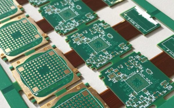
HDI PCB Design Guidelines: Optimizing High-Density Interconnect Layouts
High-density interconnect (HDI) PCBs have become a standard in modern electronics, enabling designers to create smaller, more functional devices. However, designing HDI PCBs requires careful attention to detail due to their complexity and the advanced technologies involved. This article outlines key HDI PCB design guidelines, highlights the advantages and disadvantages of HDI layouts, and provides insights into overcoming common challenges.
Key HDI PCB Design Guidelines
1. Materials and Processes
- Thinner Dielectrics: Use new, thinner dielectric materials, which may require adjustments to impedance calculations and stackup configurations.
- Solder Mask Control: Ensure tighter solder mask clearances to accommodate high-density layouts.
- Advanced Technologies: Incorporate technologies like via-in-pad and coordinate with manufacturers for optimal implementation.
- Signal Integrity: Include controlled impedance layers and appropriate reference planes to maintain signal integrity.
- Thermal Management: Design stackups to prevent hot spots and ensure even heat distribution.
2. Components
- Smaller Packages: Use components with smaller package sizes, higher pin counts, and 0.5mm pin pitches.
- Routing Strategies: Adapt routing strategies to accommodate changes in escape patterns and pin pitches.
3. Routing
- Impedance Control: Calculate impedance and manage routing constraints for transmission lines, analog signals, and power traces.
- Sensitive Routing: Use CAD tools to manage routing restrictions for sensitive areas or rooms.
- Via Types: Utilize multiple via types, including through-hole, blind, buried, and microvias. Use CAD constraint systems to manage their applications.
- Thinner Traces: Employ thinner traces for compact layouts while ensuring current capacity and signal integrity are maintained.
4. Simulation
- Design Analysis: Run simulations to validate your HDI design and ensure it meets manufacturer requirements.
- Signal Integrity Testing: Use simulation tools to analyze signal behavior and identify potential issues.
5. Vias
- Microvias and Blind/Buried Vias: Use these via types for layer transitions to save space and increase density.
- Fine-Pitch Components: Consider using fine-pitch components with smaller via diameters, but limit their depth to maintain reliability.
- Via Management: Minimize unnecessary vias to maximize routing space and reduce signal integrity issues.
- Via Filling: Use via filling for improved thermal or mechanical stability if required.
Advantages and Disadvantages of High-Density PCB Layouts
Advantages of HDI PCBs
- Miniaturization: Smaller components reduce the overall layout space, enabling compact designs.
- High-Density Circuits: Increased circuit density allows for more functionality in a smaller footprint.
- Narrow Trace Widths: Enables more traces per square inch, improving routing efficiency.
- Diverse Via Types: Enhances routing flexibility with through-hole, blind, buried, and microvias.
- Thinner Dielectrics: Reduces board thickness and improves reliability.
- Performance Enhancements: Reduces inductance, EMI susceptibility, and improves thermal management and signal integrity.
Concerns with HDI PCBs
- Layer Stackup Planning: Critical for maintaining signal integrity in high-density designs.
- Adaptive Routing Strategies: Requires new approaches due to changes in pin pitch, line width, and via types.
- Manufacturing Complexity: Involves higher costs and the need for advanced manufacturing processes and materials.
- Cost Analysis: Increased design complexity may require finding specialized manufacturers, potentially raising production costs.
- Design Research: Thorough research is essential to understand new requirements before starting HDI design.
Overcoming HDI Design Challenges
1. Layer Stackup Optimization
- Plan layer stackups carefully to ensure signal integrity and thermal performance.
- Use simulation tools to validate stackup designs before manufacturing.
2. Advanced Routing Techniques
- Employ auto-routing and manual routing strategies to manage high-density layouts.
- Use differential pair routing for high-speed signals to minimize crosstalk and EMI.
3. Collaboration with Manufacturers
- Work closely with manufacturers to ensure design feasibility and address potential manufacturing challenges.
- Leverage their expertise in advanced materials and processes.
4. Thermal Management
- Incorporate thermal vias, heat sinks, and copper pours to manage heat dissipation.
- Use thermal simulation tools to identify and mitigate hot spots.
5. Signal Integrity Analysis
- Perform signal integrity analysis to identify and resolve issues such as reflections, crosstalk, and impedance mismatches.
- Use simulation tools to optimize trace lengths and routing paths.
HDI PCB design offers significant advantages in terms of miniaturization, increased functionality, and improved performance. However, it also presents challenges such as complex routing, advanced manufacturing requirements, and higher costs. By following HDI PCB design guidelines, leveraging simulation tools, and collaborating with experienced manufacturers, designers can overcome these challenges and create high-performance, reliable HDI PCBs.