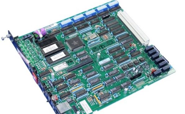
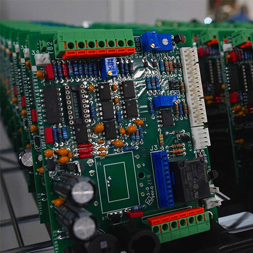
Guide to Restoring Circuit Diagrams from Physical PCBs
Often, products come without a circuit schematic, making it challenging to understand the PCB’s functionality and design principles. When faced with such a situation, follow these steps to reverse-engineer and restore the circuit diagram. This guide provides detailed instructions for accurately translating a physical PCB back into a schematic diagram.
Steps to Restore a Circuit Diagram from a PCB
1. Identify Key Reference Components
Select large or complex components, such as integrated circuits (ICs), transformers, and transistors, to serve as reference points in your drawing. Start from their pins and trace connections outward, which helps minimize errors in identifying connections and layout.
2. Leverage Component Markings
If the PCB includes component numbering (e.g., VD870, R330, C466), use these markings to your advantage:
- Components with similar initial numbers belong to the same functional unit.
- Recognizing these units aids in organizing the schematic by function, reducing confusion and improving accuracy.
3. Manually Number Components
If no component numbering is present, create a numbering system:
- Number each component for easier tracking and proofreading.
- Manufacturers often arrange related components together by functional units to minimize copper foil routing. Look for clustering as an indicator of related functionality.
4. Distinguish Power, Ground, and Signal Lines
Correctly identifying power, ground, and signal lines is crucial. To do this:
- Power Line: In power circuits, the positive end of the rectifier (connected to the power transformer secondary) often indicates the power line.
- Ground Line: The ground line typically has the largest copper foil area to minimize interference, especially in high-frequency circuits.
- Signal Line: These lines usually have the narrowest copper traces.
In mixed analog-digital circuits, ground lines are often split into separate networks. Use this distinction for added clarity.

5. Organize for Clarity
Avoid excessive crossings or intersecting lines by using terminal markings and ground symbols liberally. For complex circuits, consider drawing each functional unit separately, then combine them into a complete diagram.
6. Use Tracing Techniques for Sketching
Use transparent tracing paper and color-coded pens to map each line type (e.g., power, ground, signal) and component. Modify and deepen colors as needed to emphasize clarity, making the sketch easy to understand at a glance.
7. Familiarize with Common Circuit Units
Many circuit layouts share common units, such as rectifiers, regulators, and operational amplifiers. Draw these known units first to establish a framework, allowing faster progress with less room for error.
8. Utilize Similar Circuit Diagrams
Find and reference diagrams from similar products to accelerate your work. This approach can provide valuable insight into likely layouts, saving time and effort by avoiding guesswork.
KKPCB conducts research on special processing technologies such as ordinary double-sided boards, thick copper circuit boards, high-frequency circuit boards, HDI circuit boards, rigid-flexible circuit boards, FPC flexible boards, buried blind hole circuit boards, and IC carrier boards. Provides PCB design, PCB layout, PCB prototyping and PCB assembly services.


