Flexible PCB Manufacturing Process: Flexible Circuit Board (FPC)
Flexible PCB or Flexible Printed Circuit Boards (FPCBs) play a crucial role in modern electronics, offering flexibility, space-saving benefits, and reliability in a wide range of applications. In this article, we’ll explore the manufacturing process of flexible PCBs, from design to assembly, and discuss their diverse applications in electronic devices.
What is a Flexible PCB (FPCB)?
A flexible printed circuit board (FPCB) is a type of PCB that can be bent or twisted to fit into specific spaces or conform to different shapes. Unlike rigid PCBs, FPCBs are made from flexible materials, such as polyimide, and are ideal for use in compact, complex, and high-performance electronic devices.
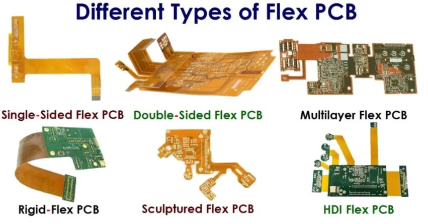
Types of Flexible PCBs
- Single-Sided Flexible PCB
- Structure: Features a conductive layer on a single flexible dielectric substrate.
- Advantages: Simple design for circuits that require minimal connections.
- Applications: Commonly used in LCD displays, cameras, and automotive dashboards.
- Double-Sided Flexible PCB
- Structure: Contains two conductive layers separated by a dielectric layer.
- Advantages: Enhanced routing capabilities and PCB design flexibility.
- Applications: Suitable for more complex circuits in smartphones and medical devices.
- Multilayer Flexible PCB
- Structure: Contains three or more conductive layers, with insulating layers between them.
- Advantages: High-density design with improved electrical performance.
- Applications: Common in aerospace, military equipment, and advanced medical devices.
- Rigid-Flex PCB
- Structure: A combination of rigid and flexible parts.
- Advantages: Durability and design flexibility in compact spaces.
- Applications: Used in wearable devices, laptops, and aerospace technologies.
- Engraved Flexible PCB
- Structure: Features varying thicknesses, allowing integration of SMD components.
- Advantages: Ideal for customized, space-constrained applications.
- Applications: Used in high-reliability industries like aerospace and automotive.
- HDI Flexible PCB
- Structure: High-density interconnect design for high-performance devices.
- Advantages: Supports fine lines, microvias, and high-pin count components.
- Applications: Essential for modern electronics such as smartphones, tablets, and IoT devices.
Flexible PCB Manufacturing Process Step-by-Step
1. Flexible PCB Design Process
- Software Tools: CAD software such as Altium Designer, Eagle, or KiCAD is used for design.
- Design Rules: Ensure compliance with standard rules like minimum trace width, spacing, and layer counts.
- Stackup: Define the number of layers, materials, and thickness.
- Gerber Files: Generate Gerber files, which are the standard format for PCB design.
Design Parameters Overview:
- Software Tools: Altium Designer, Eagle, KiCAD
- Minimum Line Width: Typically 0.1 mm or as per manufacturer capabilities
- Layers: Single-sided, double-sided, or multilayer
- Material: Polyimide or PET (Polyethylene Terephthalate)
2. Material Selection
- Substrate Material: Polyimide is commonly used for its flexibility and thermal stability.
- Copper Clad: A thin layer of copper is laminated onto the substrate.
- Adhesive: Copper is bonded to the substrate using special adhesives.
Material Properties:
- Polyimide: High flexibility, excellent thermal stability
- PET: Cost-effective, suitable for non-complex designs
- Adhesive (Acrylic): Strong adhesion, suitable for high-temperature applications
3. Circuit Patterning
- Photoresist Application: A light-sensitive photoresist is applied to the copper-clad substrate.
- Exposure: UV light exposure hardens the photoresist in the desired pattern.
- Etching: The unexposed areas are etched away, leaving the copper circuit pattern.
Patterning Process:
- Photoresist Application: Applied to copper-clad substrate
- UV Exposure: Photomask used to harden the resist in the desired areas
- Etching: Removal of unexposed photoresist, leaving copper traces
4. Lamination and Delamination
- Single-Layer FPC: Typically involves a single copper layer on a polyimide substrate.
- Multi-Layer FPC: Multiple layers are laminated together using adhesive and heat.
- Cover Layer: A protective layer (cover film) is applied to shield the circuit.
Lamination and Layering:
- Single Layer: One copper layer on a polyimide substrate
- Dual Layer: Two copper layers with a polyimide core
- Multilayer: Multiple layers pressed together
- Cover Film: Protective polyimide film covering the circuit
5. Drilling and Hole Plating
- Drilling: Precision drills create holes for vias, pads, and through-hole components.
- Plating: Copper plating over drilled holes forms electrical connections between layers.
Drilling Types and Purposes:
- Through-Hole: Connects layers in multilayer FPCs or makes electrical connections between layers.
6. Solder Mask and Surface Finish
- Solder Mask: A protective layer to prevent solder bridging during assembly.
- Surface Finish: Various finishes include ENIG (Electroless Nickel Immersion Gold), HASL (Hot Air Solder Leveling), and OSP (Organic Solderability Preservative).
Surface Treatment Overview:
- Immersion Gold: Gold over nickel for fine-pitch components
- Hot Air Solder Leveling (HASL): Cost-effective tin-lead or lead-free solder
- OSP: Organic coating for short-term protection
7. Flexible PCB Assembly Process
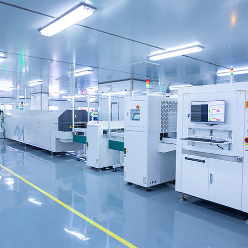
- Component Placement: Automated machines precisely place components on the flexible PCB.
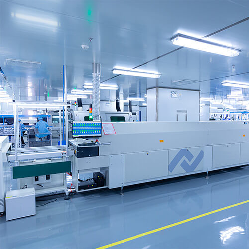
- Reflow Soldering: The PCB passes through a reflow oven, where solder paste melts to form electrical connections.
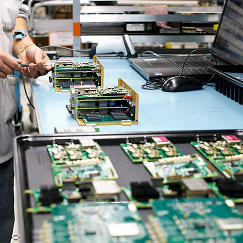
- Inspection and Testing: Optical and electrical tests ensure the PCB functions properly.
Assembly Steps:
- Component Placement: Automated, accurate component placement using placement machines.
- Reflow Soldering: Melts solder paste to form electrical connections.
- Testing: Optical and electrical inspections, along with functional testing.
Applications of Flexible PCBs
Flexible PCBs are highly versatile and used across many industries:
- Consumer Electronics: Smartphones, wearables, and cameras.
- Automotive: Used in airbag systems, GPS devices, and infotainment systems.
- Medical Devices: Found in hearing aids, pacemakers, and diagnostic equipment.
- Aerospace: Essential for satellites, communication equipment, and navigation systems.
Flexible PCBs are indispensable in modern electronics, providing flexibility, durability, and space efficiency. By understanding the flexible PCB manufacturing process from design to assembly, we can create high-quality, efficient products. As the demand for compact, reliable electronics continues to rise, flexible PCBs will play an increasingly important role in a wide array of applications
Author

