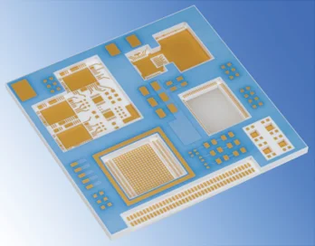
Features of KLC Series (LTCC Substrate)
Low dielectric loss characteristics (tan δ) and low resistance conductors, low electrical loss, suitable for high-frequency applications
Due to our unique manufacturing technology, the size and characteristics of each production batch and within each batch vary little
High-density wiring is achieved by improving stacking alignment accuracy
Precise control of substrate thickness and cavity shape
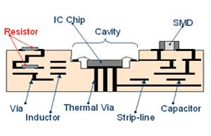
Resistance, inductance, and capacitance functions are built into the substrate and package
High-frequency applications
LTCC substrate is a type of ceramic multilayer substrate. Compared with high-temperature fired ceramic substrates (HTCC substrates) with alumina and Ag as the main components, its firing temperature is lower. In addition, as the inner conductor, Ag with low conductor resistance is used. Its electrical characteristics are as follows.

Low dielectric loss (tan δ)
Low conductor resistance)
Low dielectric loss and low conductor resistance make the electrical loss at high frequencies low, the dielectric loss is lower than that of resin substrates, and the conductor conductivity is better than that of HTCC substrates, which is generally the most suitable choice for high-frequency applications.
Millimeter wave module
In high-frequency fields such as millimeter waves, LTCC substrates have the advantage of easy lamination than fluororesin substrates.
It also has the following benefits:
Since the thermal expansion coefficient is close to that of silicon, Si-based semiconductor bare chips can be easily mounted.
Thermal conductivity is one-digit higher than that of fluororesin substrates, and heat dissipation is good
Since it does not absorb water, it has high moisture resistance
High-precision cavity molding enables miniaturization
The above characteristics indicate that LTCC substrates are suitable for semiconductor mounting, modules, and packaging in the millimeter wave band.
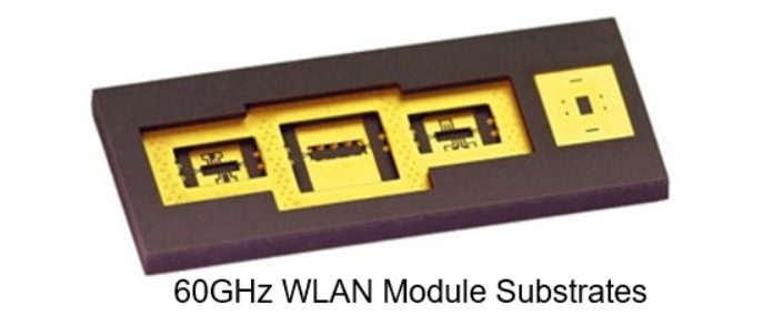
Packaging cavity formation
The cavity refers to the hollow space formed on the substrate for mounting components such as semiconductors and sensors. The cavity contributes to the miniaturization of the module and the improvement of its characteristics. KOA’s LTCC has the characteristics of high cavity size accuracy and the ability to form complex cavity shapes. In addition, the positioning accuracy of the pads for component mounting is high, which is suitable for flip-chip mounting. Complex cavity shapes for multi-chip packaging are also supported.
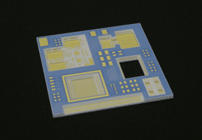
Improving heat dissipation through thermal vias
For semiconductor chips with large heat generation, heat dissipation holes can be formed directly below them to improve thermal conductivity and heat dissipation.

Formation of inner layer L, C, R
Inductors, capacitors, and resistors can be printed on the surface and inner layers. As the circuits are highly integrated, the environmental resistance of the module is improved.
Applications requiring high reliability: no outgassing
LTCC substrates are made by firing substrates composed of all inorganic components at a high temperature of more than 800°C. Since there is no outgassing, it is suitable for use in environments where outgassing is a concern, such as vacuum or high-temperature areas.

