How Single-Sided and Double-Sided PCB Assemblies Are Made
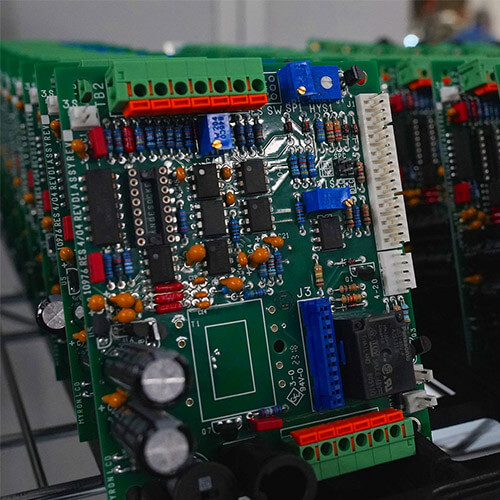
Electronic devices cannot function without PCBs, making them indispensable in the technology sector. To choose the most suitable PCB, it is crucial to understand the differences between single-sided and double-sided PCB assemblies. This guide explores both types, their processes, and their applications to help you make an informed choice.
What is a Single-Sided PCB?
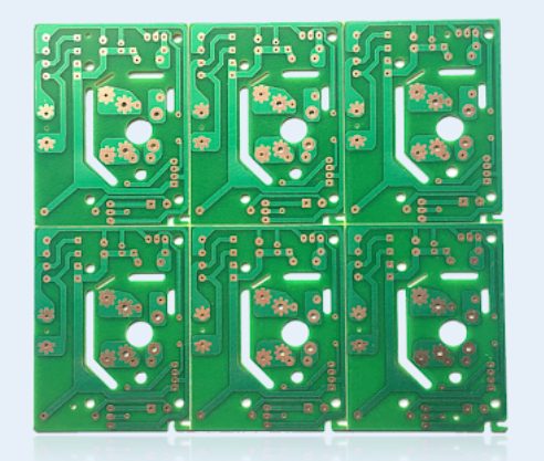
Single-sided PCBs have conductive copper traces and components mounted on one side, while the other side integrates various electronic components. They are simple to manufacture and cost-effective, making them ideal for everyday applications.
Applications of Single-Sided PCBs
Single-sided PCBs are commonly found in mass-produced devices due to their affordability. Applications include:
- Camera technology
- Amplifiers
- Energy devices
- Calculators
- Printers
- Monitors
Advantages of Single-Sided PCBs
- Cost-effective production: Simple design makes manufacturing economical.
- Ideal for low-density designs: Suitable for less complex circuits.
- Fast production rate: Less complexity leads to quicker manufacturing.
- Versatile use: Applicable in a wide range of electronic devices.
How to Design a Single-Sided PCB
Designing a single-sided PCB involves:
- Schematic Design: Create a simple circuit schematic.
- Routing Rules: Define routing parameters to ensure proper connections.
- Component Placement: Organize components to optimize trace lengths.
- Generate PCB Layout: Convert schematic to PCB design using CAD software.
Structure of a Single-Sided PCB
A single-sided PCB consists of:
- Pads: Metal holes for soldering component pins.
- Copper traces: Connect component pins electrically.
- Vias: Optional holes for connections in advanced designs.
- Boundary: Defines board size.
What is a Double-Sided PCB?
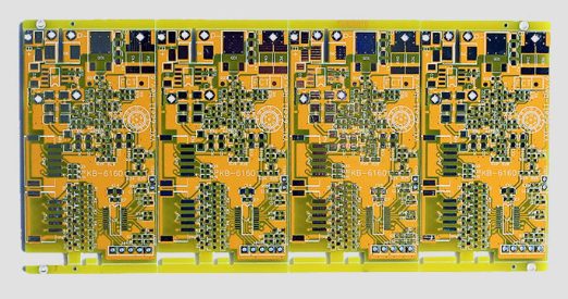
Double-sided PCBs have conductive copper and components on both sides, allowing for more complex designs. These PCBs use vias to connect the top and bottom layers, enabling higher circuit density.
Applications of Double-Sided PCBs
Double-sided PCBs are popular for advanced electronic products, including:
- LED lighting systems
- Amplifiers
- Car dashboards
- Industrial controls
- Telecommunications devices
Advantages of Double-Sided PCBs
- Higher circuit density: Components can be placed on both sides.
- Improved flexibility: Allows for complex designs and additional connections.
- Space-efficient: Reduces board size while increasing functionality.
- Cost-effective for advanced applications: Offers a good balance between complexity and performance.
How to Assemble a Double-Sided PCB
The assembly process includes:
- Soldering Side A: Apply and solder components on the first side.
- Flip the Board: Assemble and solder components on the second side.
- Inspection and Testing: Ensure quality through electrical testing.
Key Differences Between Single-Sided and Double-Sided PCBs
| Feature | Single-Sided PCB | Double-Sided PCB |
|---|---|---|
| Design | Components and traces on one side only. | Components and traces on both sides. |
| Complexity | Simpler design, limited to basic circuits. | More complex, suitable for advanced designs. |
| Manufacturing | Easier, with fewer processing steps. | Requires additional steps like via plating. |
| Cost | Lower manufacturing cost. | Higher due to complexity and materials. |
| Applications | Basic devices (calculators, remote controls). | Advanced devices (LED systems, telecom). |
PCB Manufacturing Processes
Single-Sided PCB Process
- Cutting: Prepare copper-clad laminate.
- Drilling: Create holes for components.
- Etching: Remove excess copper to define traces.
- Solder Masking: Apply protective solder mask layer.
- Silkscreen Printing: Add labels and markings.
- Inspection: Check for defects.
Double-Sided PCB Process
- Drilling and Plating: Add vias to connect layers.
- Copper Deposition: Enhance conductivity.
- Circuit Etching: Define traces on both sides.
- Solder Masking: Protect the board surface.
- Assembly: Mount and solder components on both sides.
- Testing: Perform electrical tests for continuity.
Single-sided and double-sided PCBs serve different purposes based on complexity and application needs. Single-sided PCBs are cost-effective and ideal for simpler designs, while double-sided PCBs provide flexibility and higher circuit density for advanced devices. By understanding these distinctions, you can select the best PCB type for your project.

