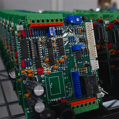
Fabrication Guidelines for RT-duroid® 5870 and 5880 High-Frequency Circuit Materials
RT-duroid® 5870 and 5880 are high-performance laminates with exceptional electrical properties, making them ideal for high-frequency and microwave applications. These materials are PTFE-based composites with excellent dielectric uniformity and low loss, reinforced with glass microfiber for mechanical stability. Proper fabrication techniques are essential to preserve their properties and ensure reliable performance.
1. Material Overview
Key Features
- Dielectric Constant (ϵr\epsilon_rϵr):
- 5870: ϵr=2.33±0.02\epsilon_r = 2.33 \pm 0.02ϵr=2.33±0.02
- 5880: ϵr=2.20±0.02\epsilon_r = 2.20 \pm 0.02ϵr=2.20±0.02
- Loss Tangent:
- Extremely low, ideal for high-frequency applications.
- Thermal Stability:
- Suitable for operating temperatures up to 260°C.
- Moisture Absorption:
- Negligible, ensuring consistent performance in humid environments.
Applications
- Microwave antennas
- Power amplifiers
- Satellite communication systems
- Radar systems
2. Handling Guidelines
- Storage:
- Store laminates flat in a clean, dry environment.
- Avoid prolonged exposure to UV light or high humidity.
- Cleaning:
- Use isopropyl alcohol or other non-aggressive solvents to clean the surface before processing.
- Handling Precautions:
- Avoid bending or twisting to prevent stress-induced warping.
3. Drilling
- Drill Selection:
- Use carbide or diamond-coated drill bits to minimize tool wear and ensure clean holes.
- Drill Speed and Feed Rate:
- High-speed drilling with low feed rates is recommended to prevent delamination.
- Typical parameters:
- Speed: 20,000–30,000 RPM
- Feed: 0.5–1.5 inches per minute (IPM)
- Hole Quality:
- Inspect for burrs, debris, or delamination.
- Use an air blast or vacuum for debris removal.
4. Etching
- Copper Cladding:
- Standard copper cladding is available in various thicknesses (e.g., ½ oz, 1 oz).
- Etching Process:
- Use standard chemical etching solutions compatible with PTFE.
- Ensure uniform etching to maintain dimensional stability and circuit integrity.
- Post-Etch Cleaning:
- Neutralize residual etchants to prevent long-term degradation.
5. Lamination
- Layer Bonding:
- For multilayer designs, use compatible bonding films (e.g., Rogers 3001 Bondply).
- Maintain uniform pressure and temperature during lamination to avoid air pockets.
- Temperature and Pressure:
- Typical lamination temperature: 200–220°C.
- Pressure: 200–300 psi, depending on stack thickness.
- Cool-Down:
- Cool gradually to minimize internal stress.
6. Soldering
- Temperature Control:
- RT-duroid® materials can withstand soldering temperatures up to 260°C.
- Avoid prolonged exposure to high temperatures to prevent degradation.
- Lead-Free Soldering:
- Compatible with lead-free processes, but rapid heating and cooling profiles are recommended to reduce stress.
7. Routing and Cutting
- Tooling:
- Use diamond-coated or carbide tools for precision cutting.
- Parameters:
- High-speed routing with minimal feed rates prevents edge chipping.
- Deburring:
- Inspect and remove burrs using non-aggressive methods.
8. Testing and Quality Assurance
- Electrical Testing:
- Measure key parameters such as dielectric constant, loss tangent, and impedance.
- Mechanical Inspection:
- Check for warping, delamination, and hole integrity.
- Environmental Testing:
- Assess performance under thermal cycling and humidity exposure.
9. Summary of Key Guidelines
| Process | Recommendation |
|---|---|
| Drilling | High-speed drilling with carbide or diamond-coated bits. |
| Etching | Use standard solutions; neutralize residual chemicals. |
| Lamination | Maintain uniform pressure and temperature during bonding. |
| Soldering | Avoid prolonged exposure above 260°C; use rapid profiles. |
| Routing | Employ high-speed, precision tools to prevent edge chipping. |
10. Practical Tips
- Minimize Tool Wear:
- Regularly inspect and replace drill bits and cutting tools.
- Impedance Control:
- Simulate and verify circuit designs to ensure consistency with target impedance.
- Environmental Considerations:
- Protect against contamination during fabrication to maintain dielectric integrity.


