Essential Checkpoints for Final Stages of PCB Design
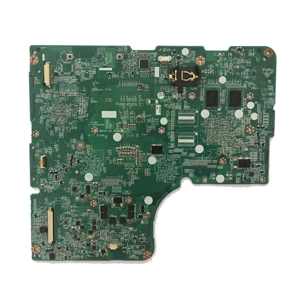
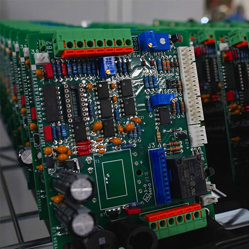
Inexperienced PCB designers often overlook critical checks in the later design stages, leading to issues like inadequate line width, misplaced silkscreens, and insufficient spacing near sockets. These errors can cause electrical or manufacturing issues, potentially requiring redesigns and increasing production costs. Below is a comprehensive list of essential PCB design checkpoints to ensure product quality and manufacturability.
1. Component Package Validation
(1) Pad Spacing
For new components, create custom packages to ensure correct spacing for optimal soldering.
(2) Via Sizing
Via sizes for through-hole components should provide enough margin, ideally no less than 0.2 mm, for proper fit and assembly.
(3)丝网印刷轮廓
将元件轮廓设计得比实际元件尺寸稍大,以便顺利安装并获得清晰的可见性。
2. PCB Layout Guidelines
(1) Distance from Board Edge
Avoid placing ICs and sensitive components too close to the board edges to minimize potential damage.
(2) Group Functional Modules
Position components of the same module together, such as placing decoupling capacitors near IC power pins, to streamline functionality.
(3) Socket Positioning
Arrange sockets based on installation requirements, generally near board edges for easy access.
(4) Socket Orientation
Orient sockets with external connections facing outward to prevent custom cable redesigns.
(5) Observe Keep Out Areas
Ensure no components are placed in Keep Out zones to avoid clearance issues.
(6) Isolate Interference Sources
Place high-speed clocks and high-current signals away from sensitive circuits like analog and reset circuits, using ground planes for separation.

3. PCB Routing Considerations
(1) Line Width Selection
Choose line width based on current-carrying requirements and manufacturer specifications; use the rule of 1mm per amp for appropriate width.
(2) Differential Pairs
For differential lines (e.g., USB, Ethernet), maintain equal length, parallelism, and consistent spacing to control impedance.
(3) High-Speed Return Paths
High-speed traces can radiate EMI if the return path is not optimized. Route high-speed lines close to their return paths, utilizing ground and power planes for reduced electromagnetic interference.
(4) Analog Signal Isolation
Keep analog signal traces away from digital signals and interference sources. Shorten analog routes to minimize noise and improve signal integrity.
4. EMC and Signal Integrity (SI)
(1) Termination Resistors
For high-speed or long digital lines, add termination resistors to reduce signal reflections.
(2) Input Signal Capacitors
For interface input signals, use a small capacitor (e.g., 330pF for low-speed signals) to filter noise, placed near the interface to maintain signal integrity.
(3) Driver Capability
Use transistor drivers for high-current signals and buffer drivers for high fan-out buses to maintain performance.
5. Silkscreen Printing
(1) Key Information
Include board name, date, and part number (PN code) for identification.
(2) Pin and Signal Labels
Label important pins and signals, especially for connectors and arrays, for easy identification.
(3)元件编号
仔细放置元件编号,避免与过孔或焊盘重叠。密集区域的编号应分组,以提高可读性。
6. Mark Points for Automated Soldering
For machine soldering, include two to three alignment mark points on the PCB to support accurate placement.
- EMC in PCB design, silkscreen placement guidelines, machine soldering alignment points
By addressing these PCB design checkpoints, engineers can greatly reduce the risk of production errors and ensure a high-quality, manufacturable PCB design.


