Electromagnetic Compatibility (EMC) Design in PCB Boards
As electronic products become more advanced, they encounter more sources of electromagnetic interference (EMI) that can disrupt device function and potentially harm health. This guide explores strategies for designing PCB boards with optimized electromagnetic compatibility (EMC), focusing on reducing interference and increasing product resilience.
1. PCB Board Design
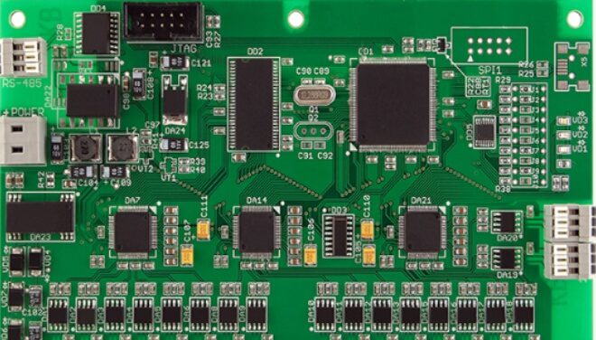
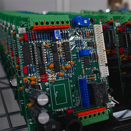
PCB boards are essential components in electronic devices, providing both structural support and electrical connections for circuit elements. The complexity and density of modern PCBs make them increasingly susceptible to interference, so careful design is critical for ensuring that devices function reliably.
1.1 Optimizing PCB Layer Design
- Layer Selection: Choose a suitable number of layers based on circuit complexity. Multi-layer PCBs significantly reduce interference and noise compared to two-layer designs, though higher-layer boards are costlier. Using a grid-like routing structure—perpendicular wiring between adjacent layers—also reduces signal interference.
- Layer Orientation: Route traces in opposite directions on adjacent layers, for example, horizontal traces on one layer and vertical traces on the next, to further reduce interference.
1.2 Optimal PCB Size
- Size Management: Balance PCB size to optimize trace lengths, impedance, and noise resistance without compromising heat dissipation. A size of 150mm x 200mm is generally recommended for mechanical durability.

2. PCB Component Layout
The arrangement of components on a PCB influences its electromagnetic compatibility. Poor component placement can result in signal radiation and crosstalk, leading to EMC issues.
2.1 Component Arrangement
- Proximity and Segregation: Arrange related components close together to reduce trace lengths and interference. Separate analog, digital, and power circuits to minimize signal coupling and EMI, and isolate high-frequency circuits from low-frequency circuits if possible.
- Noise-Prone Components: Position noisy components, such as clocks and relays, away from sensitive circuits and other logic elements.
2.2 General Layout Guidelines
- Minimizing Signal Coupling: Design component layouts to minimize signal overlap and keep low-level circuits away from high-level signals.
- Clock Components: Place oscillators, clock circuits, and processors near each other to minimize noise.
- Thermal Management: Space out high-power and heat-generating components to prevent overheating and premature component aging, especially near capacitors.
3. PCB Routing
High-frequency signals can produce distributed inductance and capacitance that interfere with PCB performance. A well-planned routing layout mitigates interference effects and improves overall signal integrity.
3.1 Routing Best Practices
- Trace Spacing and Length: Space traces to minimize capacitive crosstalk. Keep parallel signal lines apart or use orthogonal routing to reduce parasitic coupling.
- Avoid Right Angles: Use 45° angles in high-frequency trace routing to limit signal reflection and emissions.
- Isolating High-Current and High-Voltage Traces: Place high-power and high-frequency traces away from sensitive analog and digital circuits, and separate high- and low-voltage paths to prevent unwanted coupling and maintain safety.
3.2 Minimizing Antenna Effects
- Via Reduction: Limit vias to reduce inductive effects, as each via adds approximately 0.5pF of capacitance.
- Decoupling Capacitors: Place decoupling capacitors close to each integrated circuit and add bypass capacitors near electrolytic capacitors to filter high-frequency noise.
4. Circuit Design in PCB Boards
Beyond PCB layout, designing circuits with EMC in mind is crucial. Some common EMC measures include adjusting resistors and capacitors and ensuring unused inputs are grounded.
4.1 EMI Suppression Techniques
- Series Resistors: Place resistors in series along signal paths to control signal edge rates.
- Relay and Signal Filtering: Add high-frequency capacitors or diodes to dampen relay noise, and use filters on noisy signal inputs.
- Unused Gate Connections: Ground unused inputs to prevent floating states, which can introduce noise.
4.2 Filtering and Decoupling
- Input Signal Filtering: Add filters to signals entering the PCB to reduce interference from external sources.
- Decoupling Capacitors: Use high-frequency capacitors near ICs and large tantalum capacitors on power lines to provide stable power filtering.
By following these PCB design principles, you can enhance the EMC performance of electronic products, reducing interference and ensuring stable device operation across varied environments.
As a leading PCB manufacturer, members of our printed circuit board (PCB) design service team are practical partners working with you on every project and can help you achieve your goals at any time. They can complement your engineering expertise, which helps speed up time to market, reduce the time from concept to production, and ensure that quality is integrated into the manufacturing process to maximize your profits.


