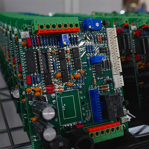
Effective Strategies for PCB Panelization
Handling small circuit boards during automated assembly can lead to defects and inefficiencies. To overcome this challenge, PCB panelization—the process of creating PCB panels from smaller boards—plays a vital role. This technique not only ensures improved handling during assembly but also reduces costs and minimizes defects. Here’s a comprehensive guide to panelizing PCBs, including methods, techniques, and best practices for successful implementation.
What Are PCB Panels?
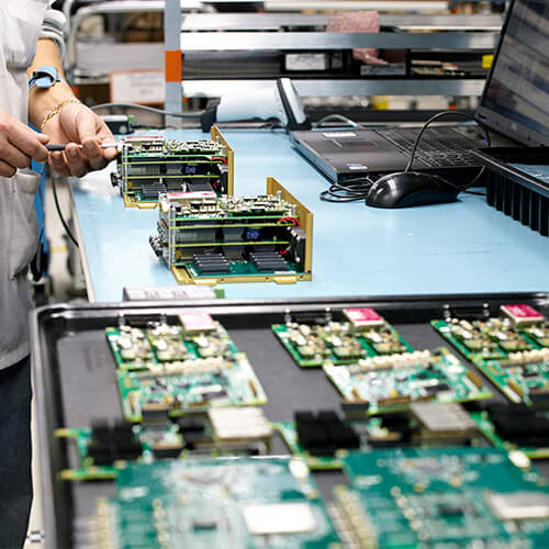
PCB Panelization, also called PCB arrays, are composed of multiple small boards arranged to form a larger unit. These panels streamline manufacturing and assembly processes. After the components are mounted, a depaneling process separates individual PCBs from the array.
Key Benefits of PCB Panelization:
- Reduced Handling Errors: Panelization improves stability during automated assembly, reducing the risk of defects.
- Cost-Effectiveness: Shared tooling and streamlined processes lower production costs.
- Enhanced Efficiency: Simplified machine programming and reduced assembly time.
Factors Influencing Panelization
- Design
- Ensure proper edge clearance and spacing between components.
- Avoid edge-hanging parts that could interfere with breakout processes.
- Components
- Account for precision parts and connectors to select the best panelization and breakout method.
- Use robust designs for fragile or sensitive components.
- Material
- Choose materials that withstand breakout forces without damage.
- Consider board thickness—thicker boards are less prone to breaking during depaneling.
PCB Panelization Methods
1. V-Panelization (V-Scoring)
- Overview: Creates V-shaped grooves to reduce board thickness by approximately one-third.
- Advantages: Precise depaneling with minimal damage to components.
- Considerations: Requires machine-based depaneling; not suitable for all .
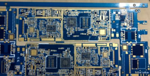
2. Tab-and-Route Panelization
- Overview: Pre-cuts PCBs and connects them to the panel with perforated tabs.
- Advantages: Flexible and supports edge-hanging component designs. Can often be depaneled by hand.
- Considerations: Tabs may leave remnants, requiring additional cleaning.
3. Solid Tab Panelization
- Overview: Uses solid tabs for extra strength and support.
- Advantages: Provides added structural integrity.
- Considerations: Depaneling requires specialized tools such as laser cutters or routers. Dust and vibration can be a concern, and laser cutters may struggle with boards thicker than 1mm.
Panelization Techniques
V-Scoring
- Best for uniform, simple designs.
- Uses angled blades to create grooves for controlled separation.
- Ideal for boards with fewer edge components.
Tab-and-Route
- Suitable for irregularly shaped PCBs or edge-hanging designs.
- Perforated tabs make manual or machine-based depaneling easy.
- Commonly used for PCBs with high component density near edges.
Solid Tab with Routing
- Offers enhanced strength for larger boards or heavy components.
- Requires precise equipment for depaneling, such as depaneling routers.
Best Practices for PCB Panelization
- Optimize Panel Size:
- Choose a panel size compatible with manufacturing and assembly equipment to reduce material wastage.
- Maintain Consistent Spacing:
- Use consistent spacing between individual PCBs to allow for efficient breakout and reduce stress on components.
- Use Fiducial Marks:
- Add fiducial marks for accurate alignment during assembly.
- Simulate Depaneling:
- Test panel designs with breakout simulations to identify weak points or potential issues.
- Collaborate with Manufacturers:
- Work closely with PCB manufacturers to determine the best methods and materials for your specific design.
PCB panelization is an indispensable process in modern electronics manufacturing. By leveraging the right methods, materials, and design principles, you can enhance production efficiency, reduce costs, and ensure defect-free assembly. Whether using V-Scoring, Tab-and-Route, or Solid Tab techniques, careful planning and execution are key to achieving optimal results.
KKPCB provides global customers with one-stop services from PCB layout, prototype PCB proofing, PCB manufacturing, PCBA processing (including SMT and DIP), PCBA testing, PCBA product assembly and outbound packaging. You could provide a Gerber file or BOM list to us, we will offer the finished PCB products or PCB assembly which are satisfied with you.
As a PCB assembly company based in China, we supply a variety of PCB electronic products to clients from different countries. We are committed to providing comprehensive PCBA solutions across various sectors. Today, many industries such as automotive, medical, consumer electronics, aerospace, digital communications, industrial control, smart home, and IoT choose our PCB assembly services.

