Detailed Explanation of PCB Manufacturing Process and Precautions
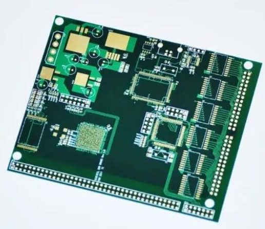
High-quality PCB production begins with high-quality design. Huaqiang PCB manufacturing heavily relies on the cooperation of the design process. Engineers, please design your PCBs according to the detailed explanation of the conventional production process below.
Design Parameters for PCB Manufacturing
1. Via (Conductive Hole)
- Minimum hole diameter: 0.3mm (12mil)
- The minimum via hole diameter is 0.3mm, and the pad size on a single side cannot be smaller than 6mil (0.153mm), preferably greater than 8mil (0.2mm).
- Hole-to-hole spacing: The distance between the hole centers (hole edge to hole edge) cannot be less than 6mil, preferably greater than 8mil.
- The distance from the pad to the outline should be at least 0.508mm (20mil).
2. Circuit (Traces)
- Minimum trace spacing: 6mil (0.153mm). The minimum spacing between traces and between a trace and a pad should not be less than 6mil. From a production perspective, the larger, the better (usually 10mil).
- Minimum trace width: 6mil (0.153mm). A trace width smaller than 6mil cannot be produced. For inner layers of multilayer boards, the minimum is 8mil.
- The spacing from the trace to the outer edge should be at least 0.508mm (20mil).
3. Pad (PTH – Pin Through Hole)
- The outer ring of the PTH pad should not be less than 0.2mm (8mil) on one side; the larger, the better.
- The hole-to-hole spacing (hole edge to hole edge) of the PTH should not be less than 0.3mm, and larger is preferred.
- The size of the PTH hole should be larger than the component pin. For a 0.6mm component pin, the hole should be at least 0.8mm to ensure proper insertion and account for manufacturing tolerance.
- The spacing between the pad and the outline should be at least 0.508mm (20mil).
4. Solder Mask
- The opening for the PTH and SMD pads should not be less than 0.1mm (4mil) on one side.
5. Character Design (Text on PCB)
- The minimum character width is 0.153mm (6mil), and the minimum character height is 0.811mm (32mil). The recommended ratio of width to height is 5:1 (e.g., a character with a width of 0.2mm and height of 1mm).

6. Non-Metallic Slots
- The minimum spacing for slots should not be less than 1.6mm, otherwise, milling the edges will become very difficult.
7. Platemaking
- Gapless and gapped panels: For gapped panels, the gap should be at least 1.6mm for a 1.6mm-thick board; otherwise, milling edges will be challenging. Gapless panels have a gap of approximately 0.5mm.
- The process edge (board margin) cannot be less than 5mm.
Precautions in PCB Design Files
1. PADS Design Files
- In double-sided board files, ensure that the hole attribute is set to Through Hole (not Blind or Buried), as this affects the generation of drilling files.
- When designing slots in PADS, avoid adding them directly with components, as GERBER generation might fail. Instead, add slots in DrillDrawing.
- PADS typically uses Hatch copper, but the manufacturer uses Flood copper laying. After moving the original file, the copper should be re-laid and saved properly to avoid short circuits.
2. PROTEL99SE and DXP Design Files
- Solder Mask: Manufacturers typically use the Solder Mask layer for the solder mask. If a solder paste layer (Paste layer) is required, it should be moved to the Solder Mask layer for proper GERBER generation.
- Do not lock the outline in Protel99SE; otherwise, GERBER files will not be generated correctly.
- Avoid selecting the KEEPOUT option in DXP files, as this will block the outline and prevent GERBER generation.
- Layer Design: The top layer should be positive, and the bottom layer should be reverse. When stacking, ensure the boards are not mirrored accidentally, especially in single-piece designs, as this could result in incorrect orientation.
3. General File Considerations
- The outline (e.g., board frame, slot, V-CUT) must be placed on the KEEPOUT or mechanical layer, not on the silk screen or circuit layers.
- If there is a discrepancy between the mechanical and KEEPOUT layers’ shapes, special instructions must be provided. Ensure the shape is valid, and delete the line segment at the intersection of the outer shape and the inner groove.
- Slots and holes designed in the mechanical layer should be treated as copper-free unless specified otherwise.
- Metalized Slots: To ensure proper processing, the safest method for creating metalized slots is to use multiple pads together.
4. Gold Finger Board
- For gold finger boards, specify whether bevel chamfering is required.
5. Final Checks
- Ensure the GERBER files have the correct number of layers, as manufacturers typically work directly from the GERBER files.
6. Gerber File Naming Convention
- Component side circuit: gtl
- Component side solder mask: gts
- Component side characters: gto
- Solder side circuit: gbl
- Solder side solder mask: gbs
- Solder side characters: gbo
- Board outline: gko
- Hole diagram: gdd
- Drilling: drll
By adhering to these guidelines, engineers can ensure their PCB designs are manufacturable and optimized for high-quality production. These precautions and design considerations help reduce production errors, improve yield, and ensure the integrity of the final product.


