Decoding High-Density Interconnect (HDI) PCB Technology: An Overview
In the evolving world of electronics, where everything matters including the size, shape and performance of a device, PCBs help in the development and implementation of complex yet advanced technologies in electronic devices day by day.
In the present world, especially in the current technological era, devices are becoming more compact and advanced. For implementing the compact and at the same time advanced electronic technology in the world, HDI PCBs contribute abundantly. It allows the integration of several complex circuitry into a simple and smaller configuration.
A phenomenal impact has been made by high density interconnect PCB in PCB production and development. Unlike conventional PCBs, where the design is of two-dimension and through-hole vias, HDI PCBs stand out by enabling large wiring density, enhanced trace width and higher layer count.
In this article, we are going to look into HDI PCBs and what impact it has on the electronic industry.
What is High Density Interconnect PCB?
High Density Interconnect (HDI) PCB is a circuit board which comprises a high wiring density per unit area. The feature of high density interconnect PCB including good spaces and lining, small vias, capture pads etc. helps in enhancing the performance of the PCB electrically. high density interconnect PCB implementation will also help in reducing the shape and size of the electronic equipment.
Using high density interconnect PCB comes with a lot of advantages and benefits like high-speed performance, high frequency and compact size. Their speciality and features find application in so many aspects including personal computers, MP3 players, gaming consoles and smartphones. They are also implemented in places where higher-layer count is required.
Laser micro-vias are one of the main things in high density interconnect PCB manufacturing, adding up with better lines and thin materials. The extra functions per unit area are achievable by the enhanced density of HDI PCBs. The structure with a high density of high density interconnect PCB will allow the routing easy for the chips with a high number of pin counts and complicated pin structure.
Extra precision is required while placing HDI on the board than conventional PCBs because of the pads’ miniaturization and fine pitch of the circuitry. The chances of mechanical shock are always low because of the smaller size and lesser weight of HDI PCBs.
Types of HDI PCB
Some of the HDI PCBs manufactured are listed below.
1. Through-Hole HDI PCB
This HDI PCB is the combination of high density interconnections with traditional through-hole vias. To achieve higher routing density, through-hole vias are incorporated with micro vias sometimes. They are usually implemented in applications where high-density routing and through-hole component compatibility need to be balanced.
2. Sequential Build-Up HDI PCB
This is the type of HDI PCB which is manufactured by laminating multiple layers of thin core materials in sequence. Each layer provides a unique circuit pattern and specifications. This type of HDI PCB helps in the formation of flexibility and layer thickness in the PCBs according to the specific requirements. They are also known as multi-layer build-up HDI PCBs.
3. Rigid-flex HDI PCB
In these PCBs, there are both rigid and flexible areas which are mainly interconnected by microvias. This special feature of rigid-flex HDI helps in places where three-dimensional routing and lightweight designs are in great requirement. They also utilise the benefit of combining HDI technology with the flexibility of flex PCBs or circuits.
4. Any-Layer HDI PCB
This is the PCB that extends into multiple layers with the help of microvias. This allows connection between layers in any combination. They also offer maximum flexibility in routing and interconnectivity because of the limited restriction on the interconnection of layers. They are highly applicable in high-performance applications which require strict signal integrity. They are also known as stacked micro vias or stack vias HDI PCBs.
5. Build-Up HDI PCB
Their speciality is a coreless structure which utilises thin dielectric layers and copper for the construction. Then with the help of microvias, they form the circuitry. They are referred to as coreless HDI PCBs.
6. Cavity-Based HDI PCB
In this HDI PCB, they include cavities in the board itself in the structure to incorporate components and connections. The purpose of this cavity is to help in the miniaturization and integration of components thereby introducing more streamlined designs for the PCBs. They are highly applicable in areas where space management is crucial.
Features of High Density Interconnect PCB
Some highlighted features of high density interconnect PCBs are listed below:
- More Layers
The layer count of high density interconnect PCB is always more than two. They usually range from four to ten layers sometimes even more than ten. These layers give us the advantage of producing more options for routing and it also helps in the vias placement within the board. This will thus result in increasing the overall wiring density of the board.
- Microvias
Microvias allow the coupling of traces between multiple layers of the PCB without the need for large drill sizes, resulting in denser routing and finer-grade components. high density interconnect PCBs make use of these microvias and these microvias are tiny plated-through holes with a width of less than 150 micrometers.
- Buried and Blind Vias
high density interconnect PCBs can include blind vias in addition to traditional through-hole vias. In blind vias, the connection is typically made in an outer layer to one or more inner layers. On the other hand, there are also buried vias which connect the inner layer and there is no penetration through the board thickness. In both vias, they help in reducing signal interference and they also help in enabling extra complex configurations in routing.
- Enhanced integrity of signals
In high density interconnect PCBs, there is always only a small amount of electromagnetic interference and signal distortion. This is mainly because of the use of vias such as micro vias, blind vias and buried vias. The usage of these vias in HDI will enhance the integrity of signals in radio frequency as well as digital applications which require high speed.
Advantages of HDI PCB
- High component density
This PCB can withstand a high number of components in a limited area. This will help in reducing the overall size of the electronic devices where HDI boards are implemented. For devices like smartphones, wearable electronics, and smart gadgets, it is pretty useful where the availability of space is compact and limited.
- Improved Electrical Performance
HDI PCB uses some advanced technologies in the time of its manufacturing. The techniques used in manufacturing including microvias, buried vias and blind vias will help the PCB in improving the electrical performance, lowering the impedance and increasing the power distribution.
- Cost-effective
Compared with the advanced manufacturing process. It may seem pretty expensive than regular PCBs but in the long run, HDI PCBs are good enough for electronic devices in cost cutting. Due to its compact design and high component density, the material used will be less resulting in reducing overall reduction cost.
- Flexible Design
One of the main features that HDI PCB has is its flexibility in design. Their flexibility will allow design engineers to create innovative products in the industry. This will also help the HDI PCBs in clean routing, finding accurate trace width and spacing, increase layer count.
- Increased performance
Implementing HDI PCBs in the electronic world has opened the gate for several innovative and exclusive applications including high-speed computing, Network management, Avionics, Defence etc. The enhanced performance that this PCB has offered made it applicable in such high-end power-required applications.
Disadvantages of HDI PCBs
- Complexity
Even though HDI PCBs are highly delegated and advanced in their design and working, they also have complexity in several features due to their increased layer count and complex routing methodologies. The complexity of these PCBs also results in higher engineering costs, longer time for development and a high possibility of disk error. Troubleshooting on these PCBs also requires high knowledge and expertise to take action.
- Challenges in Production
Due to the advanced manufacturing procedure followed in HDI PCB, it is sometimes very challenging to implement and work out. The specialized procedures used in their manufacturing including microvia drilling, laser ablation and lamination procedures will require very specialized equipment, materials and highly skilled workers for the production which might not be available and affordable readily. The complexity will also increase the defects in the PCBs while manufacturing and it will end up having lower production and a higher quantity of scrap leftovers.
- Concerns in reliability
The use of micro vias and buried vias in HDI will bring u some issues related to reliability. Sometimes, the usage of these vias will lead to via-cracking, fatigue in solder joints and challenges in heat dissipation. To achieve long-term reliability, we must consider the material to be selected, the manufacturing process and environmental factors during the manufacturing process.
- Design compel
The design of HDI PCBs offers great flexibility in their designs due to their higher component density and compact size. However, this flexibility put some design constraints on HDI PCBs. These constraints limit the options attainable to engineers and designers in HDI PCB manufacturing.
Applications of HDI PCBs
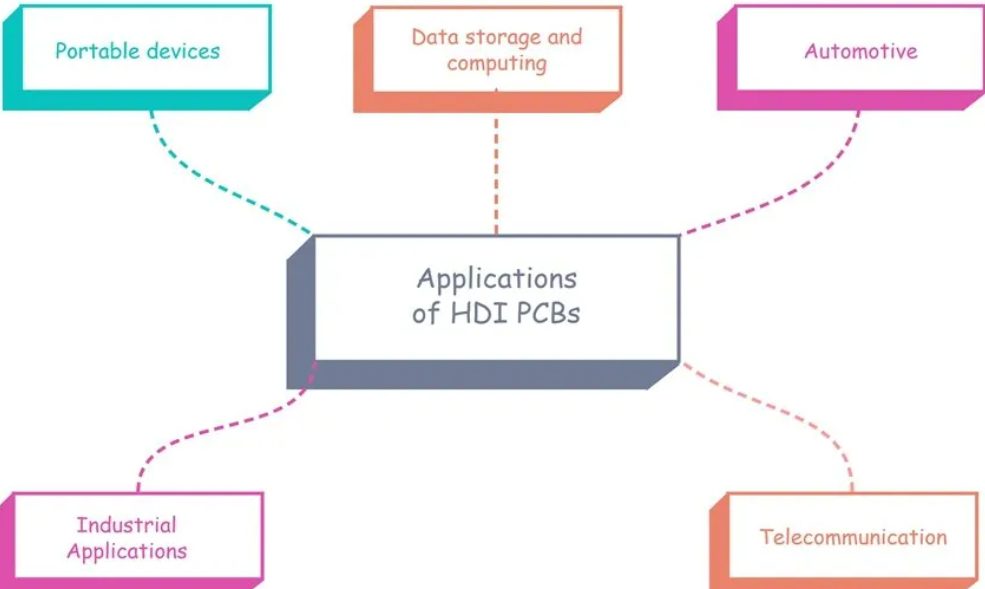
- Portable devices
Due to the ability of HDI PCBs to densely pack components in a small area and their compact size, they are extensively used in applications such as smartphones, wearable electronics, tablets etc. Even though it is small in size and design, HDI PCBs deliver high performance and functionality.
- Data storage and computing
Using HDI PCBs on data storage devices and computing systems which require high performance will benefit by achieving high processing speed, and improving signal strength and integrity. HDI helps in the integration of complex circuits and dense memory modules.
- Automotive
Modern vehicles highly use electronic systems in their assembly. HDI PCBs nowadays are incorporated in so many applications in automotive including infotainment, GPS, auto drive assistance and the overall safety of vehicles. The typical applications in automotive such as Collision Avoidance systems, cruise control, ABS and infotainment systems have a huge implementation of HDI PCB.
- Industrial Applications
In the automation industry and robotic systems, we need to use compact yet sophisticated electronic technologies for high-end industrial production and manufacturing. The usage of HDI PCBs helps in the integration of sensors, actuators and communication interfaces in industrial devices.
- Telecommunication
The communication protocol including the base station, routers, transmitters network devices etc. rely on HDI PCBs for better performance and enhanced communication. It helps in enabling the transmission of data at a high rate, improved signal processing and overall wireless communication. This results in a reduced footprint.
Manufacturing of HDI PCBs
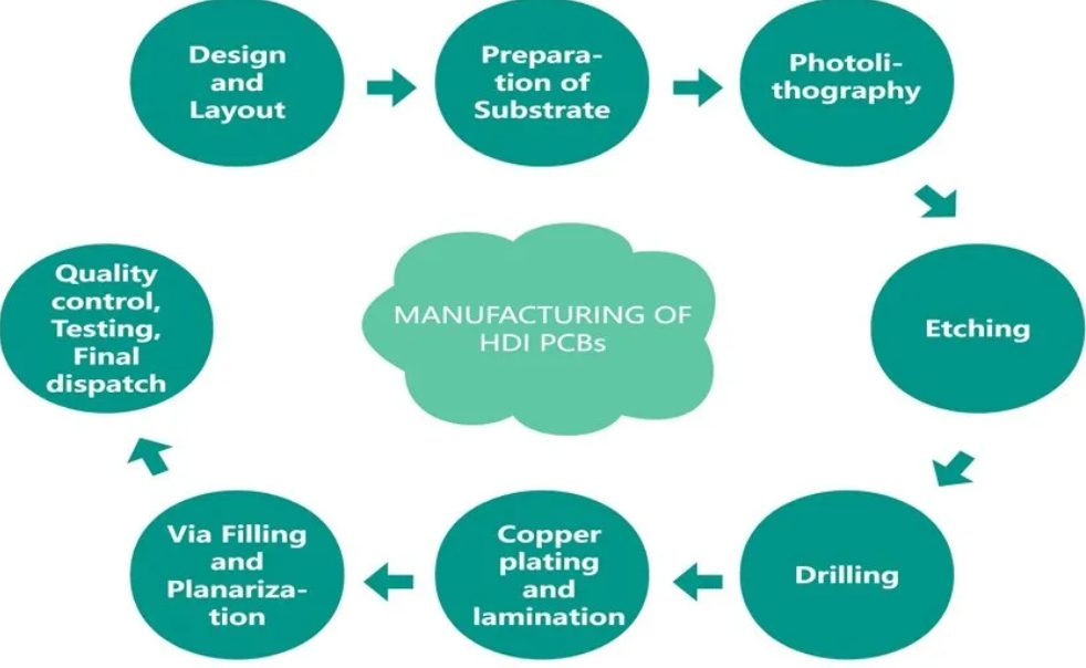
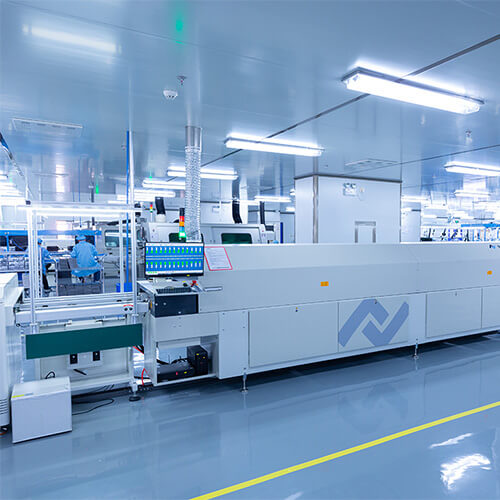
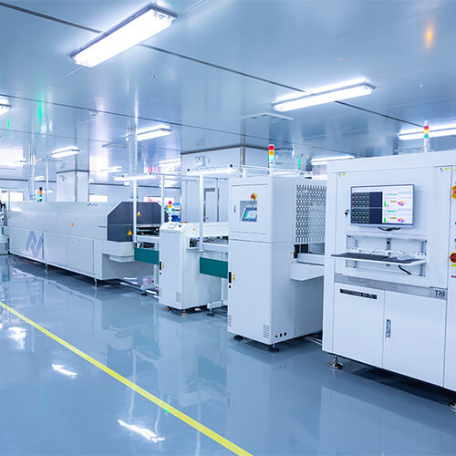
The manufacturing process of HDI PCBs involves several steps. Similar to normal PCBs, HDI PCBs will also offer some advanced manufacturing techniques. The complexity and compactness of HDI PCBs can be achieved by the following manufacturing process.
- Design and Layout
For creating the design and final layout of the HDI PCBs, we use specific software tools and specialized equipment. To get the desired layout and design, the examination is carefully conducted in the placement of components and routing of the PCB. This careful examination is done due to the high density interconnections in HDI PCBs.
- Preparation of Substrate
Generally, FR-4 (Flame Retardant 4) is the substrate material used in the manufacturing process of HDI PCBs. The process is carried out by cleaning the substrate and removing the unwanted materials in it.
- Photolithography
This is an unavoidable process in PCB manufacturing. This process involves placing a photosensitive material (Photoresist) on the surface of the substrate. The PCB design is used as a photo mask and UV light is passed through it to transfer the desired pattern to the substrate. This process is also called Imaging.
- Etching
Like any other PCB manufacturing, HDI PCBs also go through a process known as etching. This process is a chemical process and it involves the removal of extra copper which leaves with the pattern traces.
- Drilling
The drilling is the next step initiated in order to place the components and secure the connections in the inner layer of PCBs. HDI PCBs utilise laser drilling with less than 150-micrometre diameter holes. Holes these small will help in proper interconnection in HDI PCBs.
- Copper plating and lamination
Copper plating is done with the help of electroplating in the PCB surface. The placement of copper in the inner and outer layers will help enhance the interconnection within the PCB and result in increasing the overall conductivity of the board.
Lamination is the process of bonding the inner layer and outer layer of the PCB with heat and pressure. After the process, we are left with solid PCBs with multiple layers bonded to form a single layer.
- Via Filling and Planarization
HDI PCBs will do vias filling and this process has steps like copper deposition, filling of conductive paste and resin filling. This is usually carried out in high density interconnect PCB manufacturing to enhance its reliability. After vias filling is done, another technique called planarization is carried out to remove excess material from the previous process. This technique involves mechanical milling and chemical polishing.
- Surface Finish
As a final step, a surface finish is applied on the board to protect the copper traces and to increase the overall dependability of the PCB. Some commonly used surface finishes in high density interconnect PCB manufacturing are:
- ENIG (electroless nickel immersion gold)
- OSP (Organic Solderability preservatives)
- Immersion silver
- Quality control, Testing and Final dispatch
After going through all the manufacturing procedures. The high density interconnect PCB is left with the final testing and quality checking. This ensures that the PCB manufactured is fault-free and ready to be used by the customer. Only after this process, the final dispatch of the finished product is done.
In summary, HDI PCBs contribute to the advancement of electronic manufacturing by miniaturization and optimizing the performance of the board. The numerous advantages including improving the electrical performance, effectively utilizing the space, enhancing the reliability and increasing the flexibility of designs, make this model of PCB a good and reliable technology.
The usage of advanced manufacturing techniques like micro vias, blind vias, and buried vias helps designers reduce the complications in design and helps them pack more devices into a smaller footprint. This advancement in technology finds application in smartphones, electronic gadgets, wearables and many other advanced applications. As technology evolves, HDI PCB is going to remain an unavoidable trend and technology in the electronic industry.

