Copper Foils for High Frequency circuit board Materials
Rolled copper is made by successive cold rolling operations to reduce thickness and extend length starting with a billet of pure copper. The surface smoothness depends on the rolling mill condition.
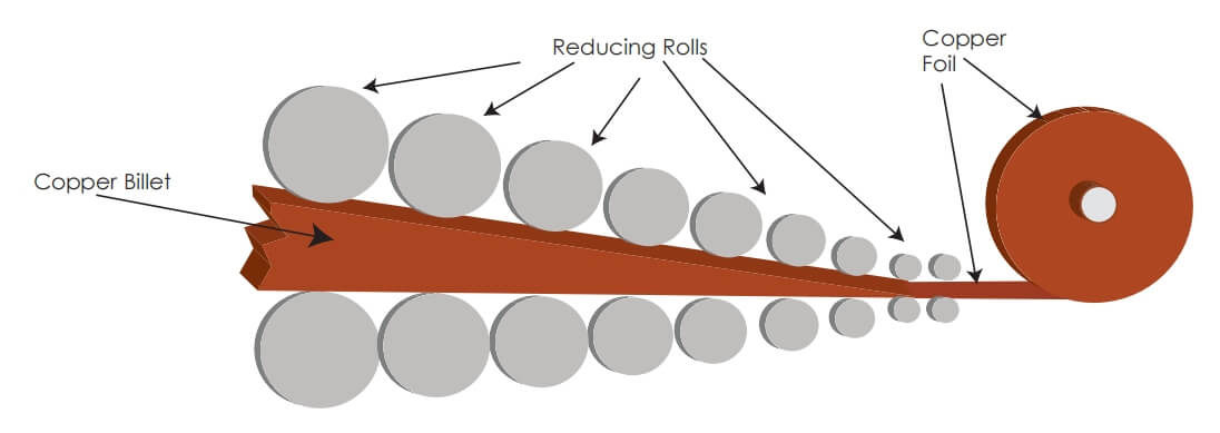
Fig. Electrodeposited Copper Manufacturing Process
Resistive Copper
The matte side of the ED copper is coated with metal or alloy that acts as a resistive layer. The next process is to roughen the resistive layer with nickel particles.
Reverse Treated ED Copper and LoPro Copper Foil
Reverse treated foils involve the treatment of the smooth side of electrodeposited copper. Treatment layers are thin coatings that improve adhesion of the base foil to dielectrics and add corrosion resistance which makes the shiny side rougher than it was before. During the process of making circuit board panels, the treated side of copper is laminated to the dielectric material. The fact that the treated drum side is rougher than the other side constitutes a greater adhesion to the dielectric. That is the major advantage over the standard ED copper. The matte side doesn’t need any mechanical or chemical treatment before applying photoresist. It is already rough enough for good laminate resist adhesion.
In case of the LoPro™ copper, a thin layer of adhesive is applied on the reverse treated side of the copper. There is a physical layer of the bond enhancement material. Just like the reverse treated electrodeposited copper, the adhesive treated side is bonded to the dielectric layer for better adhesion. Our RO4000 series material are available laminated with LoPro copper foil.
Crystalline Structure
Electrodeposited copper crystals tend to grow lengthwise in the Z-axis of the foil. Typically, a polished cross-section of electrodeposited copper foil has the appearance of a picket fence, with long crystal boundaries perpendicular to the foil plane. Rolled copper crystals are broken and crushed during the cold rolling operation. They are smaller than the electrodeposited crystals, and have irregular, spherical shapes, nearly parallel to the foil plane.
Copper Foil Roughness Measurements
Surface roughness can be measured by mechanical and optical methods. Many sources report the “Rz” (peak to valley”) profile as measured by a mechanical profilometer . However, in our experience, the Sq (RMS) profile as measured by white light interferometry of the treated side of copper foil correlates best with conductor losses. Figure 1 shows the interferometer profile of the ½ oz. ED foil used on Rogers’ PTFE and TMM laminates. Table 1 shows the types of copper foils used on Rogers’ laminate materials along with typical profile information. A recent study (reference 7) has shown that the “top side” profile has a very different structure than the treated side and has very little effect on conductor loss, even in a stripline configuration.
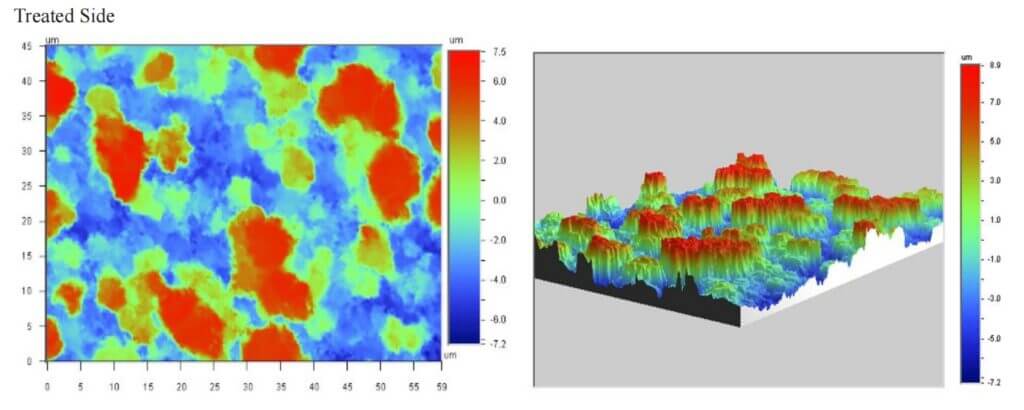

Fig 1. Surface topographies of ½ oz electrodeposited foil by white light interferometry
As displayed on Table 1, roughness data of electrodeposited and rolled copper foils with different thicknesses was obtained by using an optical surface profiler. It also shows for which products the individual copper foils are used at Rogers Corporation. The rolled copper with no surface treatment is typically the smoothest.
|
Foil Type |
Weight or Thickness | Surface Roughness(1) Sq (μm) | Products | ||||||||||||||||||||||||
| Dielectric Side |
Top Side |
||||||||||||||||||||||||||
| Rolled | 1 oz (35 μm) | 0.4 | 0.3 | XtremeSpeed™ RO1200™, RO3003™, RO3035™, RT/duroid® 5870, 5880, 6002, 6202, CLTETM, CLTE-ATTM, CLTE-XTTM, CLTE-MWTM, CuClad®217, CuClad 233, CuClad 250, DiClad®527, DiClad®870, DiClad®880, IsoClad®917, IsoClad 933 |
|||||||||||||||||||||||
| ½ oz. (18 μm) | 0.4 | 0.3 | |||||||||||||||||||||||||
| Electrodeposited | 2 oz (70 μm) | 1.6 | 0.4 | TC350TM, TC600TM , AD250TM, AD255TM, AD300TM, AD350TM | |||||||||||||||||||||||
| 1 oz (35 μm) | 1.5 | 0.4 | |||||||||||||||||||||||||
| ½ oz. (18 μm) | 1.6 | 0.4 | |||||||||||||||||||||||||
| 2 oz (70 μm) | 3.0 | 0.4 | CuClad 217, CuClad 233, CuClad 250, DiClad 527, DiClad 870, DiClad 880, IsoClad 917, IsoClad 933, CuClad, CLTE, CLTE-AT, CLTE-XT, CLTE-MW, AD1000TM |
||||||||||||||||||||||||
| 1 oz (35 μm) | 1.7 | 0.4 | |||||||||||||||||||||||||
| ½ oz. (18 μm) | 1.5 | 0.4 | |||||||||||||||||||||||||
| 1 oz (35 μm) | 2.4 | 0.4 | RO3003, RO3006, RO3010, RO3035, RO3210, RT/duroid 5870, 5880, 5880LZ, 6002, 6035HTC (not available with 1/4 oz cu) , 6202, 6006, 6010.2LM,TMM® 3,4, 6,10, 10i, 13i |
||||||||||||||||||||||||
| ½ oz. (18 μm) | 2.0 | 0.4 | |||||||||||||||||||||||||
| ¼ oz. (9 μm) | 1.3 | 0.4 | |||||||||||||||||||||||||
| 4 oz (140 μm) | 3.0 | 0.4 | 92MLTM, 92ML StaCool | ||||||||||||||||||||||||
| 3 oz (105 μm) | 3.2 | 0.4 | |||||||||||||||||||||||||
| 2 oz. (70 μm) | 3.5 | 0.4 | KappaTM 438, RO4003C™, RO4350B™, RO4360G2™ RO4533™, RO4534™, RO4535™, RO4730G3™ (½ oz & 1 oz only), RO4835TM, 92ML, 92ML StaCool, CU4000™ |
||||||||||||||||||||||||
| 1 oz. (35 μm) | 3.2 | 0.4 | |||||||||||||||||||||||||
| ½ oz. (18 μm) | 2.8 | 0.4 | |||||||||||||||||||||||||
| 1 oz. (35 μm) | 0.5 | 0.4 | XtremeSpeed RO1200, AD300D™-IM™, AD255C™-IM, DiClad 880-IM | ||||||||||||||||||||||||
| ½ oz. (18 μm) | 0.5 | 0.4 | XtremeSpeed RO1200 | ||||||||||||||||||||||||
| 2 oz. (70 μm) | – | 0.4 | RO4835TTM RO3003G2™ (½ oz & 1 oz only) |
||||||||||||||||||||||||
| 1 oz. (35 μm) | – | 0.4 | |||||||||||||||||||||||||
| ½ oz. (18 μm) | 0.7 | 0.4 | |||||||||||||||||||||||||
| Electrodeposited Low Profile Reverse Treated | 2 oz. (70 μm) | 1.0 | 2.0 | DiClad 527, DiClad 870, DiClad 880, IsoClad 917, IsoClad 933, CuClad 217, CuClad 233, CuClad 250, CLTE, CLTE-AT, CLTE-XT, CLTE-MW, AD1000, XtremeSpeed RO1200 (2 oz. only) |
|||||||||||||||||||||||
| 1 oz. (35 μm) | 1.0 | 1.3 | |||||||||||||||||||||||||
| ½ oz. (18 μm) | 1.0 | 0.8 | |||||||||||||||||||||||||
| 2 oz. (70 μm) | 1.0 | 1.8 | AD250, AD255, AD300, AD350, RT/duroid 6002, 6006, 6010.2LM, 6202, 6002PR, 6202PR, TC350, TC350 Plus, TC600 |
||||||||||||||||||||||||
| 1 oz. (35 μm) | 1.0 | 1.5 | RT/duroid 6035HTC, 6002, 6006, 6010.2LM, 6202, 6002PR, 6202PR, AD250, AD255, AD300, AD350, RO3003, RO3006, RO3010, RO3210, TC350, TC350 Plus, TC600 |
||||||||||||||||||||||||
| ½ oz. (18 μm) | 1.0 | 1.0 | |||||||||||||||||||||||||
| LoPro® Foil | 1 oz. (35 μm) | 0.9 | 1.3 | RO4003C, RO4350B, RO4533, RO4534, RO4535, RO4725JXRTM, RO4730JXR™, RO4730G3™, RO4830™, RO4835, CU4000 LoPro |
|||||||||||||||||||||||
| ½ oz. (18 μm) | 0.9 | 0.8 | |||||||||||||||||||||||||
| Resistive Foil | NiCrTicerTCR® ½ oz. (18 μm) |
1.4 | 0.4 | RO4003C, RO4350B, RO4360G2, RO4835 | |||||||||||||||||||||||
| OhmegaPly® ½ oz (18 μm) |
1.7 | 0.4 | RO4003C | ||||||||||||||||||||||||
| OhmegaPly ½ oz. (18 μm) |
1.2 | 0.4 | CuClad 217, CuClad 233, CuClad 250, CLTE, CLTE-XT, Diclad 527, DiClad 870, DiClad 880, IsoClad 917, IsoClad 933, RO3003 , RO3006, RO3010, RO3035, RO3210, RT/duroid 5870, 5880, 6002, 6202, 6006, 6010.2LM |
||||||||||||||||||||||||
Electric Performance of Laminates
It has been well-known since the earliest days of microwave engineering with wave guides that the conductor surface roughness can substantially affect the conductor loss. In 1949, S.P. Morgan
(1) published results of numerical simulations that indicated that a factor of two increase in conductor loss could becaused by surface roughness. Hammerstad and Jensen
(2), incorporated Morgan’s model, along with correlated data in microstrip design method. The H&J model became the“textbook”
(3) method for calculating the effect of surface roughness on conductor loss. More recently, at higher frequencies and with thinner laminates, it was found that H&J significantly under predicted the increase in conductor loss with surface roughness (5,6). The “Hall-Huray” model
(4), developed from a“first principles”analysis, has been recently incorporated into commercial design software. In our experience, with modest adjustments to the input parameters, the Hall Huray model can accurately predict conductor loss over a wide range of laminate thicknesses and frequencies.
The Hall-Huray model has been incorporated in Rogers Corporation’s impedance and loss calculator, MWI. We are currently working to develop the best Hall-Huray input parameters for modeling Rogers’ laminates. Please check at Rogers Technical Support Hub on-line or your Rogers Sales Engineer for updates.
Rogers copper foils studies (5,6,7) have also shown that the copper profile can affect the propagation constant, with higher profile foils leading to an apparent increase in the effective dielectric constant Figure 3 shows the calculated dielectric constant of 50 ohm TLs on 4 mil liquid crystal polymer (LCP) laminates clad with different foils with Sq values ranging from 0.4 to 2.8 microns.
The circuit with the highest profile foil exhibits an increase in DK of nearly 10%. The effect of copper profile on phase response is not accounted for in the Hall Huray model.
The effect of copper profile on insertion loss can be quite large (Fig.2). At 90 GHz, the insertion loss of a 50 ohm TL fabricated from a 0.004” thick liquid crystal polymer (LCP) laminates with RAfoil (blue line), is 2.2 dB/inch and is nearly perfectly modeled as a smooth conductor. The same substrate clad with EDfoil exhibiting with Sq value of 2.0 microns, exhibits an insertion loss of 3.7 dB/inch. Figure 4 shows the morphologies of the roughness treatments on the conductors used to generate the data presented in Figure 2.
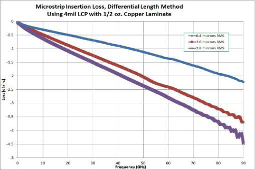

Fig 2.Comparisons of different copper roughness on the insertion loss of microstrip transmission lines
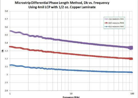
Fig 3. Comparisons of different copper roughness on the dielectric constant of microstrip transmission lines
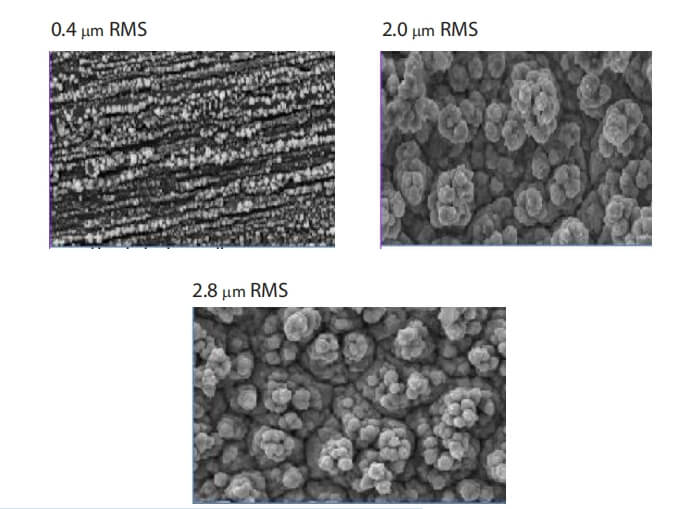
Fig. 4: SEM images of 1/2 oz copper foils – Treated Side
Mechanical Performance of Laminates
A. Thermal Shock Resistance
Under some extreme conditions of rapid thermal cycling, electrodeposited copper may exhibit thermal stress cracks in narrow conductors. Under similar conditions, rolled copper has significantly improved resistance to cracking. Although electrodeposited copper has greater tensile strength and elongation before breaking, rolled copper has better elastic elongation before reaching permanent deformation.
B. Foil Adhesion
Because the adhesion of resin systems to metals is predominantly mechanical, bond strength is directly related to the surface roughness of the treated foil side. Typical peel strengths after thermal shock for 1 oz. copper foils to.
C. Bondability of Stripline Assemblies (PTFE Substrates)
The SEM photographs below illustrate the differences in topography and roughness between copper types and etch dielectric surfaces. If the boards are to be adhesive bonded, then for electrodeposited copper, sodium etch or plasma etch of the dielectric surface is not necessary, provided that care is exercised to preserve the surface topography. However, for rolled copper-clad circuit boards, the surface roughness of the dielectric will give a poor mechanical bond, and surface treatment is necessary for reliable chemically bonded assemblies.
Properties
The different manufacturing methods of the two types of foil lead to differences in the electrical and Mechanical properties. The primary differences are listed in Table 2.
| Property | Electrodeposited | Rolled | ||||||||||||||||||||||||||
| ¼ oz 8 μm) |
0.5 oz (18 μm) |
1 oz. (35 μm) |
2 oz (70 μm) |
0.5 oz (18 μm) |
1 oz. (35 μm) |
2 oz. (70 μm) |
||||||||||||||||||||||
| Tensile Strength,kpsi | 15 | 33 | 40 | 40 | 20 | 22 | 28 | |||||||||||||||||||||
| Elongation, %* | 2 | 2 | 3 | 3 | 8 | 13 | 27 | |||||||||||||||||||||
| Vol Resistivity Mohm•cm |
1.66 | 1.62 | 1.62 | 1.78 | 1.74 | 1.74 | ||||||||||||||||||||||
Table 2. Typical Foil Properties
* Values represent properties after lamination to a PTFE laminate.
Rogers Statement on Resistive Foil Visual Appearance and Resistivity Expectations
Rogers Advanced Connectivity Solutions (ACS) produces upon request a select number of copper clad laminates using commercially available, subtractively processed resistive foils. Resistive foil technology enables the use of planar resistors within the circuit boards that are made from our laminate products. The availability of these resistive foils varies depending on each particular copper clad laminate product offered by ACS. However, in general ACS uses both OhmegaPly® foil from Ohmega Technologies, Inc. (http://ohmega.com/) and TCR® foil from Ticer Technologies (http://www.ticertechnologies.com/). ACS customers are encouraged to research the specific resistive foil products that are available as well as the performance and processing details from each foil supplier prior to placing orders with Rogers.


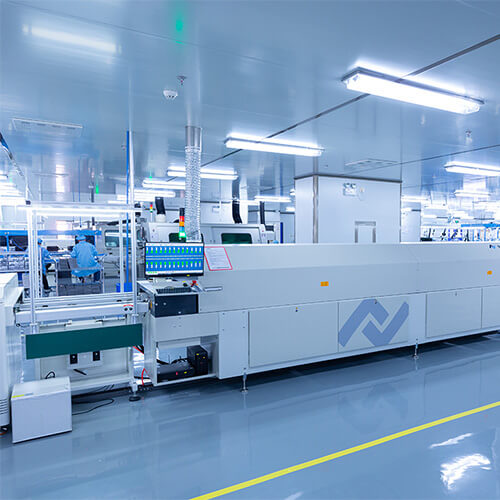

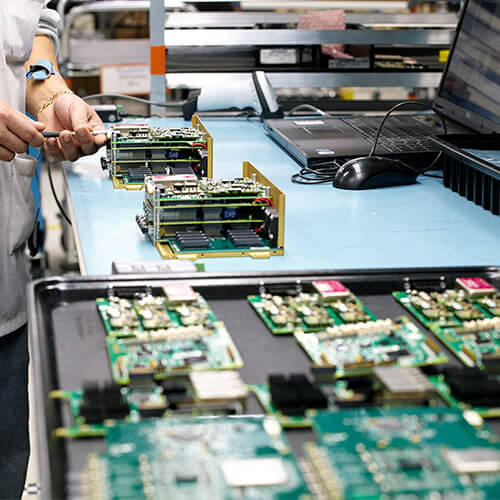
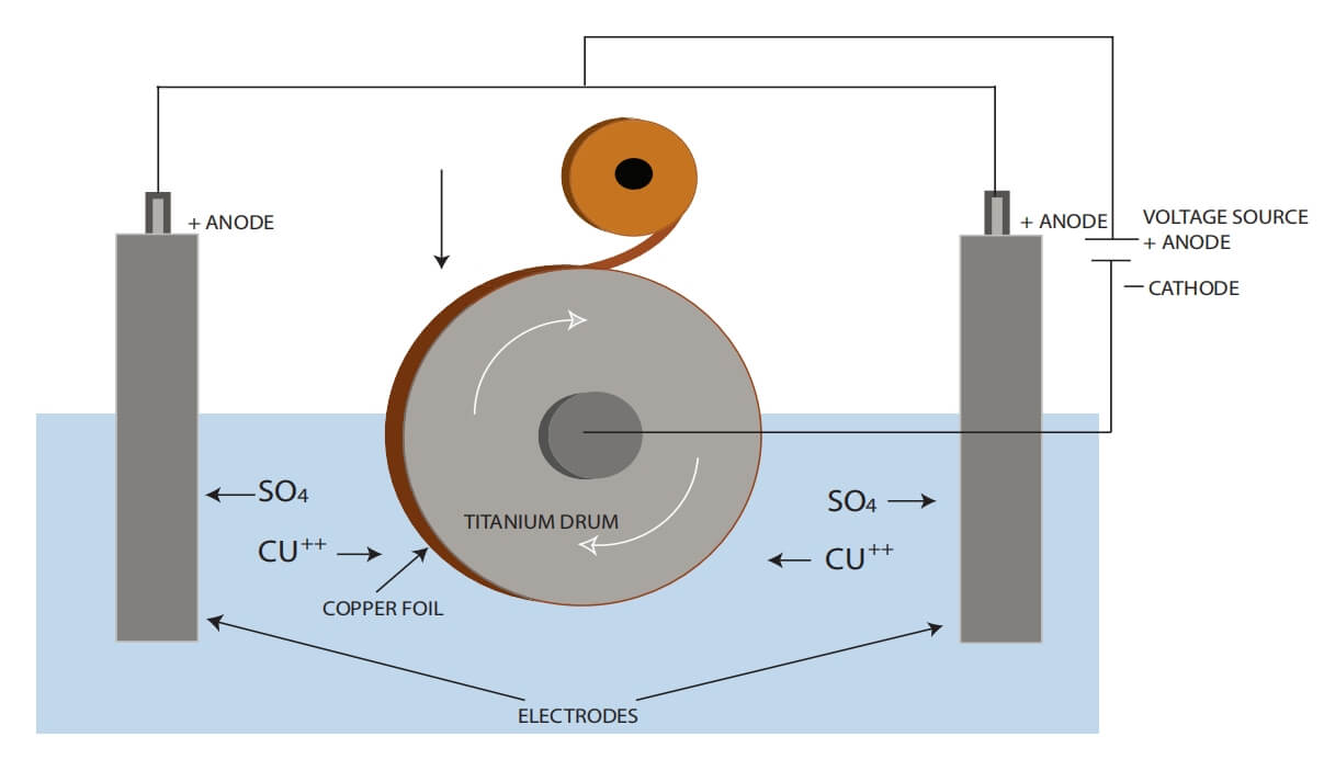 Fig. Electrodeposited Copper Manufacturing Process