Copper Foil in PCB Laminates
The Complexity of Copper Foil in the PCB Industry
Copper foil used in the PCB industry is more complex than one might imagine. Copper is not only an excellent electrical conductor but also a superb thermal conductor, making it the ideal material for most PCB applications. Understanding the various characteristics of copper foil is crucial for engineers.
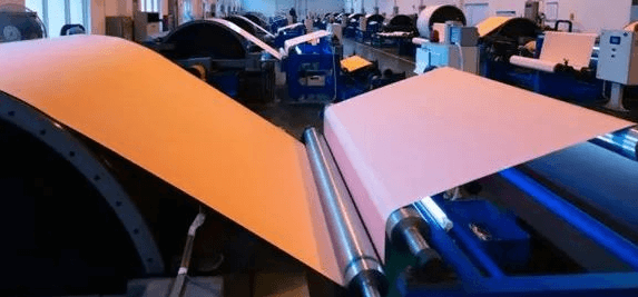
In the PCB industry, the common types of copper foil are Rolled Annealed Copper (RA) and Electrodeposited Copper (ED). The production process for RA copper foil begins with pure copper ingots, which are continuously rolled to reduce thickness until the desired foil thickness is achieved. In contrast, ED copper foil is manufactured using an electroplating process, where copper ions are deposited onto a rotating titanium drum, with the thickness of the foil being directly affected by the drum’s rotational speed. Regardless of whether it’s RA or ED copper foil, the finished product must undergo multiple processing steps.
Overview of Copper Foil in PCB Laminates
Various Processing Methods for Copper Foil
Copper foil undergoes various processing methods for several reasons. Some of these processes are passivation treatments aimed at preventing oxidation before use, while others enhance the chemical adhesion between copper foil and certain resin systems (such as PPE and PTFE). Due to the differences in resin systems, materials respond differently to various treatments, and some treatment/resin combinations yield better adhesion than others. Additionally, certain processing methods ensure proper bonding under high-temperature conditions, while others create reliable bonding surfaces to ensure long-term reliability at elevated temperatures.
For rigid PCB applications, ED copper foil is the most commonly used, although RA copper foil can also be employed. Generally speaking, RA copper foil is more expensive than ED copper foil, and it is usually only used when certain properties of RA copper foil offer a significant advantage for the application. The manufacturing process of RA copper foil results in a very smooth surface, which leads to lower insertion losses, making it well-suited for high-frequency and ultra-high-speed digital applications. Additionally, RA copper foil’s unique internal crystal structure is beneficial for applications that require circuit bending; however, this structure presents a technical drawback concerning the etching of small circuit features. Nonetheless, specific etching techniques can mitigate this issue to some extent.
ED copper foil is widely used throughout the PCB industry. It comes in various types, typically classified by surface roughness and/or processing methods. The IPC categorizes ED copper foil based on roughness into several types, including Low Profile (LP), Very Low Profile (VLP), and Extremely Low Profile (HVLP).
Methods for Measuring Copper Foil Roughness
There are multiple methods for measuring the roughness of copper foil, and differences in these methods can lead to confusion in measurement results. Generally, there are two primary methods: contact measurement and non-contact measurement. Contact measurement utilizes a physical probe (i.e., a stylus) to measure the peaks and valleys of the copper foil surface, while non-contact measurement typically involves using reflected light or lasers to ascertain the surface’s contours.
Due to differences in stylus tip size, the accuracy of contact profilometers can be lower, often failing to capture the depth of ultra-narrow roughness valleys. Furthermore, the stylus may merely “plow” over the highest points, resulting in inaccurate measurements. Experienced engineers are aware of these issues and can often make minor adjustments to alleviate accuracy problems. However, in general, non-contact profilometers are usually more accurate than contact-based ones when it comes to fine-grained copper foil.
Describing Surface Roughness Characteristics
The surface roughness characteristics of copper foil can be described in various ways. PCB manufacturing engineers typically use the Rz value to describe roughness, which indicates the peak-to-valley height measured over multiple lines in a sample area. When the Rz value is measured over an area (rather than a single line), it is referred to as Sz. The meaning of Sz is essentially the same as Rz. For high-frequency or high-speed digital (HSD) design engineers, the Rq or Sq parameters of copper foil are often needed. Rq/Sq represents the root mean square value of the roughness of multiple copper foil samples. Classical electromagnetic models show that Rq/Sq parameters can better reflect the impact of copper foil roughness on RF or HSD performance, resulting in better alignment with actual circuit performance.
Another important characteristic of surface roughness of interest in modeling is the Surface Area Index (SAI), also known as the Surface Area Ratio. It is defined as the ratio of the surface area of roughness within a scanned area to the area that is ideally flat. This roughness value can be used for specific electromagnetic model simulations, enabling the simulation results to exhibit excellent matching and accuracy with actual circuits over ultra-wide bandwidths.

