


Copper Current Density in PCB Design
Copper current density refers to the amount of continuous current going through a copper wire —whether on a circuit board as a trace or not. According to the principles of Joule or Ohmic heating (represented as VI or I²R), any material that conducts electricity will generate heat, leading to a gradual rise in temperature in both the conductor and its surrounding environment.
Considerations When Designing to Account for Copper Current Density
| Consideration | Details |
| Maximum Service Temperature | Expected operating temperature, for a standard consumer device around 45°C maximum. |
| Glass Transition Temperature (Tg) | Keep board temperature below 130°C to avoid softening and delamination for typical FR4 substrate. |
| Enclosure Temperature | Account for how hot the inside of the enclosure might become. |
| Climate Conditions | Consider environmental conditions in the regions where the board will be used. |
| Copper Thickness | Default is 35μm thick copper, with options for thicker copper if required. |
| Higher Tg Boards | Higher Tg boards are available for applications needing greater thermal stability. |
Determining Acceptable Current Density
The current density in a trace is primarily determined by thermal limitations. Similar to high-current integrated circuits, the main constraint is usually how much heat the trace will generate under the load and its ability to dissipate that heat. The temperature increase due to this thermal dissipation often becomes the critical factor that limits the current-carrying capability.
A current density calculator is a useful tool for estimating the heat generated in copper traces. When the copper area is smaller, it has a higher resistance, which causes a greater voltage drop and more heat as the current increases. Accurately calculating the current density is crucial for managing heat in your PCB design and maintaining reliable performance.
Current Density Equations
| Use the formula J=Eρ to determine the current density within the conductor. In this equation:J represents the current density in amperes per square meter (A/m²).E is the electric field’s magnitude, expressed in volts per meter (V/m) or newtons per coulomb (N/C).ρ is the resistivity of the conductor, measured in ohm meters (Ω·m). The resistivity of copper is approximately 1.68×10⁻⁸ Ω·m at room temperature (20°C). |
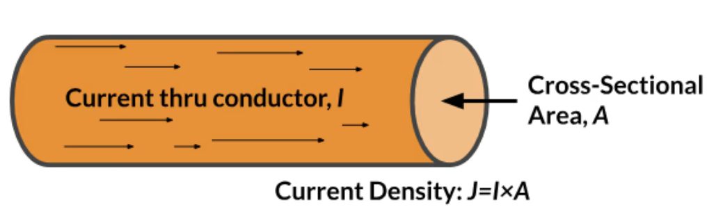
| Additionally, the current density can also be calculated using the formula J=I/A:I is the current flowing through the conductor.A is the cross-sectional area of the conductor. |
Calculators for Maximum Copper Current Density
It’s best to figure out the current your PCB’s copper traces need to carry, the maximum expected ambient temperature, and the highest temperature your trace can safely reach. Then, you can apply formulas from IPC-2221 to determine the required trace width. However, if you don’t have direct access to the IPC standards, many online trace width calculators or advanced PCB software such as OrCAD X can aid in figuring this out.
Alternatively, in the case of designing a cable, you can refer to wire gauge tables, where each wire or strand has a specific current rating. These tables provide a straightforward way to determine the current-carrying capacity of different wire sizes, saving you the trouble of manual calculations, as this data has been established long ago.
Copper Current Density for Vias
The current-carrying capacity of a via is closely linked to its cross-sectional area. A larger surface area allows for better heat dissipation, which in turn supports a higher current flow. The cross-sectional area itself depends on factors like trace thickness and width. Larger vias have a lower resistance, while smaller vias have a higher resistance. This resistance leads to heat generation within the vias.
Larger vias dissipate heat more effectively, supporting higher currents without overheating. For instance, a 12 mil (0.3mm) via can handle a little over 1A, but increasing via size doesn’t always proportionally increase current capacity; 10-12 mil is often optimal.
Via Design for High Currents
Several factors affect copper current density in vias, and in general their current-carrying capability, including its cross-sectional area, trace width, and temperature rise. Techniques like via tenting and plugging are used to boost conductivity, prevent corrosion, and protect against short circuits. Here are the maximum current ratings for plated through-hole vias in a standard PCB design:
- 0.15 mm via diameter: 0.5 A
- 0.2 mm via diameter: 0.7 A
- 0.3 mm via diameter: 1 A
- 0.4 mm via diameter: 1.5 A
- 0.5 mm via diameter: 2 A
- 0.6 mm via diameter: 2.5 A
- 0.8 mm via diameter: 4 A
- 1.0 mm via diameter: 6 A
Thin traces tend to heat up more than vias due to lower thermal conductivity, but wider traces can act as heat sinks, lowering their temperature compared to the via. Following IPC 2152 guidelines and using adequately plated vias helps prevent excessive heat buildup. Factors like plane layers and high thermal conductivity substrates also reduce conductor temperatures.
In 2009, the IPC introduced the IPC-2152 standard, which defines guidelines for the current-carrying capacity in PCB design. It provides recommendations for selecting the right sizes for internal (vias) and external conductors, considering the necessary current rating and acceptable temperature rise above the ambient level.
As a leading PCB manufacturer, members of our printed circuit board (PCB) design service team are practical partners working with you on every project and can help you achieve your goals at any time. They can complement your engineering expertise, which helps speed up time to market, reduce the time from concept to production, and ensure that quality is integrated into the manufacturing process to maximize your profits.