


Copper Current Density in PCB Design
Copper current density refers to the amount of continuous current flowing through a copper trace on a PCB. According to Joule or Ohmic heating principles (represented as VI or I²R), any conductive material generates heat, leading to a gradual temperature rise in both the conductor and its surroundings. Managing copper current density is critical to ensure reliable PCB performance and prevent overheating. This article explores key considerations, design guidelines, and tools like OrCAD X to optimize copper current density in PCB designs.
Key Considerations for Copper Current Density
| Consideration | Details |
|---|---|
| Maximum Service Temperature | Expected operating temperature, typically around 45°C for consumer devices. |
| Glass Transition Temperature (Tg) | Keep board temperature below 130°C to avoid softening and delamination for FR4 substrates. |
| Enclosure Temperature | Account for internal enclosure temperature to prevent overheating. |
| Climate Conditions | Consider environmental conditions where the PCB will operate. |
| Copper Thickness | Default is 35μm; thicker copper can be used for higher current applications. |
| Higher Tg Boards | Use higher Tg boards for applications requiring greater thermal stability. |
Determining Acceptable Current Density
The current density in a trace is primarily determined by thermal limitations. The main constraint is how much heat the trace generates under load and its ability to dissipate that heat. A current density calculator is a useful tool for estimating heat generation in copper traces. Smaller copper areas have higher resistance, leading to greater voltage drops and more heat as current increases. Accurate current density calculations are crucial for managing heat and ensuring reliable PCB performance.
Current Density Equations
- Current Density Formula:
J=EρJ=ρE- JJ: Current density (A/m²)
- EE: Electric field magnitude (V/m or N/C)
- ρρ: Resistivity of copper (1.68×10⁻⁸ Ω·m at 20°C)
- Alternative Formula:
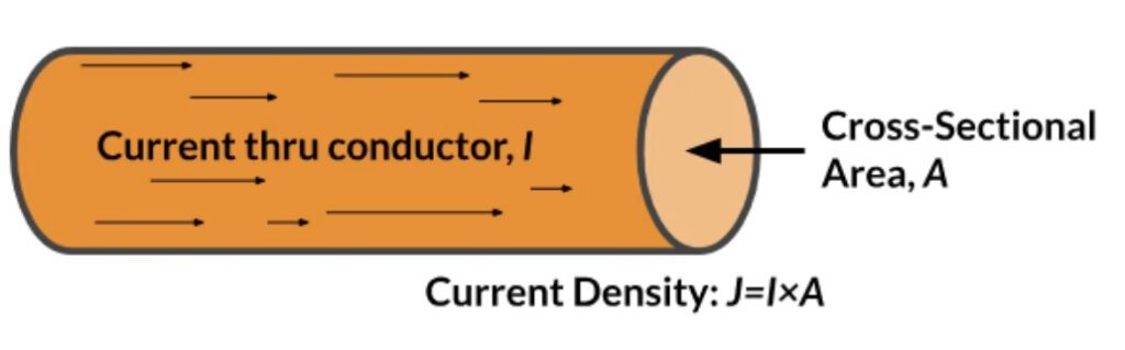
J=IAJ=AI- II: Current flowing through the conductor (A)
- AA: Cross-sectional area of the conductor (m²)
Calculators for Maximum Copper Current Density
To determine the required trace width, use formulas from IPC-2221 or online trace width calculators. Advanced PCB design software like OrCAD X can also automate these calculations. For cable designs, refer to wire gauge tables, which provide current ratings for different wire sizes.
Copper Current Density for Vias
The current-carrying capacity of a via depends on its cross-sectional area. Larger vias dissipate heat more effectively, supporting higher currents without overheating. For example:
| Via Diameter | Current Rating |
|---|---|
| 0.15 mm | 0.5 A |
| 0.2 mm | 0.7 A |
| 0.3 mm | 1 A |
| 0.4 mm | 1.5 A |
| 0.5 mm | 2 A |
| 0.6 mm | 2.5 A |
| 0.8 mm | 4 A |
| 1.0 mm | 6 A |
Via Design for High Currents
Several factors affect copper current density in vias, including cross-sectional area, trace width, and temperature rise. Techniques like via tenting and plugging enhance conductivity, prevent corrosion, and protect against short circuits. Following IPC-2152 guidelines ensures optimal via sizing and prevents excessive heat buildup.
How OrCAD X Aids in Current Density Designs
OrCAD X offers advanced features to optimize current flow and thermal performance in PCB designs. Below are some key capabilities:
| Feature | Description | How It Aids in Copper Current Density Design |
|---|---|---|
| HDI Technology | Supports blind, buried, and micro vias with constraint-driven via selection. | Optimizes via placement and size to reduce resistance and heat dissipation in high-density designs. |
| Cross-Section Editing | Enables detailed setup of PCB stack-ups, including layer thickness and materials. | Allows designers to choose appropriate materials and thickness for better heat dissipation and current handling. |
| Constraint Manager | Manages electrical, physical, and spacing constraints, including trace width. | Ensures trace widths and via sizes are optimized to handle required current levels, preventing overheating. |
Key Takeaways
- Copper current density is a critical factor in PCB design, affecting heat generation and reliability.
- Use current density calculators and IPC standards (e.g., IPC-2221, IPC-2152) to determine trace widths and via sizes.
- Optimize via design with techniques like tenting and plugging to enhance conductivity and heat dissipation.
- Leverage advanced tools like OrCAD X to streamline design processes and ensure optimal thermal performance.
By following these guidelines and utilizing tools like OrCAD X, engineers can effectively manage copper current density, ensuring reliable and efficient PCB designs.