Consumer electronics
- Home
- Consumer electronics
Consumer Electronics PCB Assembly service
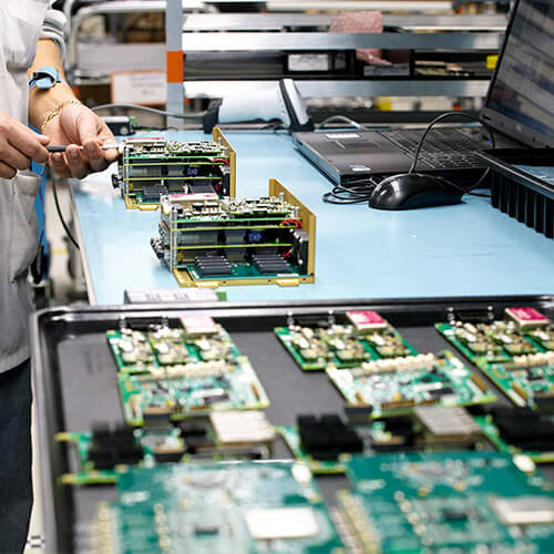
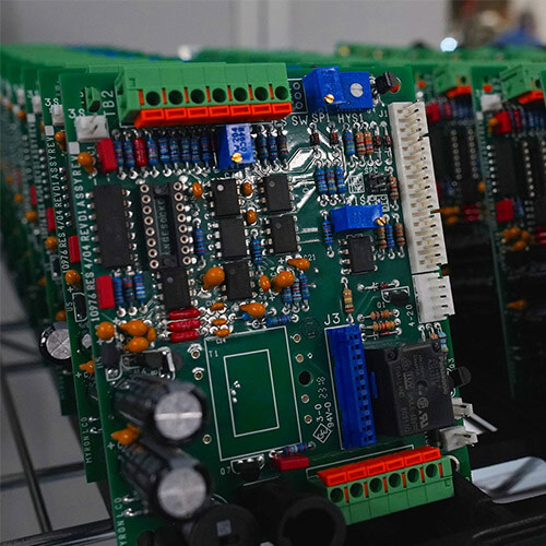
In today’s era, the need for consumer electronics PCB assembly is growing faster than the global population. All types of consumer electronic devices are made to perform our daily task faster and easy. As a consumer PCB manufacturer, we manufacture consumer electronics PCB which can be used in a wide range of modern consumer electronic devices. We manufacture high quality PCBs by following IPC class 3, RoHS and ISO certifications and regulatory standards which is important for many consumer electronics OEMs.
KKPCB, we have over 20 years of experience in crafting a wide variety of PCBs. Whether you need a PCB for a smart home device, a portable electronic or a gaming accessory, we have covered you. We are capable of understanding client requirements and can design PCBs accordingly to exceed customer expectations. We support all types of PCBs, including Rigid-flex PCB and can provide you the suggestions for the right type of PCBs for your industry. Right from design to box build services, our expert professionals have the requisite experience to offer you the best.
Why us for consumer electronics PCB
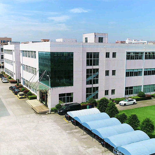
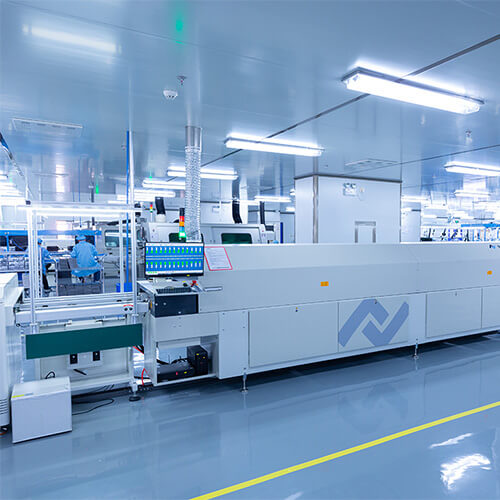
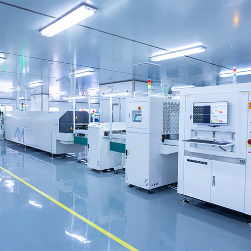
State-of-the-art facility
KKPCB, we have the necessary technology to ensure we deliver the most complex PCBs. Besides our team of experts is equipped with the industry best practices right from design to assembly.
Stringent Manufacturing Processes
In our quest to offer reliable PCBs for consumer electronics, we ensure that we adhere to industry standards and best practices. Our robust testing protocols ensure there isn’t room for any error.
Quick turnaround time
Quick go-to-market is a big source of advantage in the highly competitive consumer electronics industry. To this end, we offer quick turnaround times that enable you to launch your product that much faster.
No volume constraints
With KKPCB, you do not have to worry about the volumesof PCB that you require. From prototype quantities to large production runs we have you covered.
Consumer electronics PCB industry applications
KKPCB offers extensive PCBA, wire harness, cable, and box build assembly services for commercial and industrial markets, with a strong focus on the electric vehicle industry. Our experienced team works with customers to fully realize their electric vehicle designs, regardless of the complexity.Automotive electronics is the combination of electronic information technology and traditional automotive technology. It is the general term for body electronic control and vehicle electronic control. PCBs are widely used in automotive electronics, including power control systems, safety control systems, body electronic systems, entertainment communications, etc.

Audio Equipment and Systems
- Cell Phone
- Computer
- Smart Headphones
- Various Data Collection Wearable Devices
- Medical Related Wearable Devices
- Smart speakers
Consumer medical devices
KKPCB provides consumer product electronics manufacturing services covering all stages of product development. Includes PCB design and manufacturing, prototyping, testing, assembly and packaging. Our expertise ensures seamless execution of projects from concept to delivery.
- Orthotics
- Oxygen concentrator
- Cervical and lumbar traction device
- Electronic thermometer
- Blood glucose monitor
- Blood pressure monitor
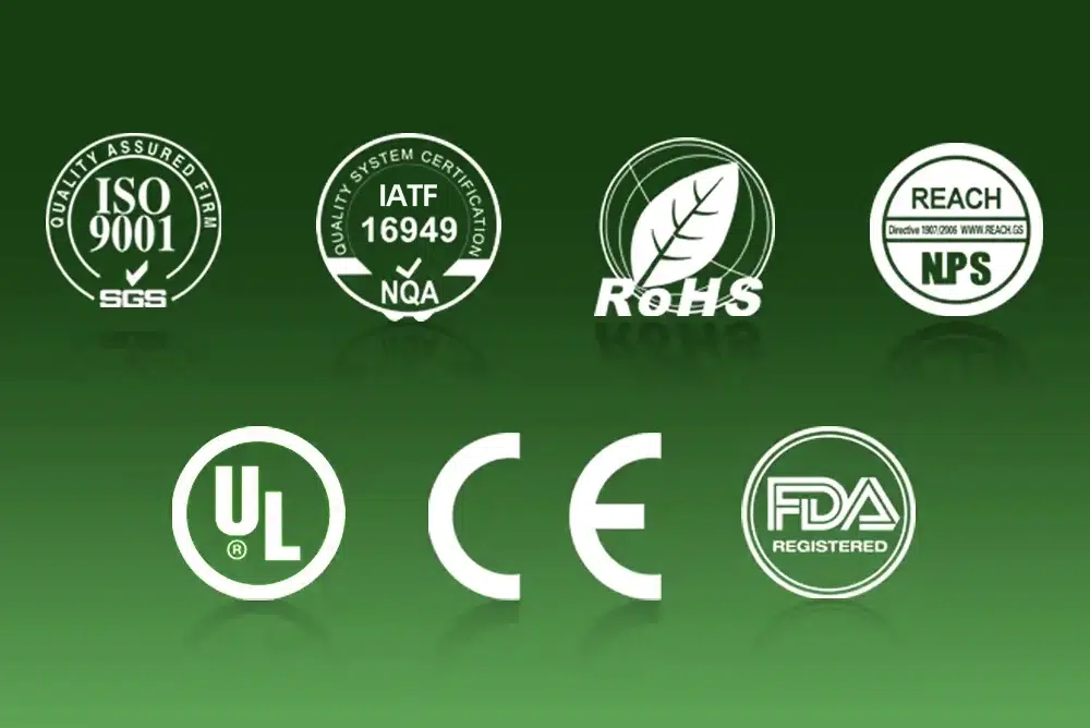
Core Certification
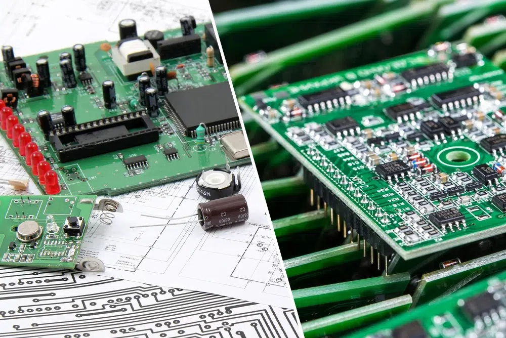
We adhere to strict quality control measures and follow industry standards and regulations in Consumer Electronic to provide products that meet or exceed customer expectations.
- IS0 9001
- IS0 13485
- IS0 14001
- IATF 16949
- ROHS
- REACH
- UL
- PDA
Consumer Electronics PCB Manufacturing Process
The various stages of PCB manufacturing span:
1. Electronics PCB Design and Output
To begin with, a PCB layer is created using a PCB design software by designers. Once the design is approved for production, the design is exported into a supportive format. A Design for Manufacturability test is run to ensure that the design fulfills the requirements for minimum tolerances. What follows next is the PCB printing process.
2. Printing the inner layers
The film is next printed onto a copper foil. The basic form of PCB is a laminate board whose core material is epoxy resin and glass fiber. The laminate serves as an ideal body for receiving the copper. The substrate material provides a sturdy and dust-resistant starting point for the PCB. Copper is pre-bonded on both sides. The process involves whittling away the copper to reveal the design from the films.
3. The copper
sided laminate is cleaned and the clean panel receives the photo resist layer, which hardens after exposure to UV light. The light passes through the clear parts of the film, hardening the photo resist on the copper underneath. The areas not meant to harden are then slated for removal.
4. Removing the Unwanted Copper
A powerful chemical preparation is used to eat away the excess copper. While the exposed copper is removed, the desired copper remains protected beneath the layer of photo resist.
5. Layer Alignment and Optical Inspection
The inner layers are now aligned to the outer ones. With the help of an optical punch, holes are accurately punched. An Automatic Optical Inspection is carried out to ensure absence of defects. Once the stage of inspection is passed, the PCB moves to the final stages of production.
6. Layer-up and Bond
All the layers are now fused. A prepreg layer is placed over the alignment basin. The substrate layer fits over the prepreg before placing the copper sheet. More sheets of prepreg sit on top of the copper layer. Finally, an aluminum foil and copper press plate complete the stack. Now it’s prepped for pressing.
7. Drill
Holes are now are bored into the stack board. An x-ray locator identifies the drill target spots.
8. Plating and Copper Deposition
After drilling, the panel moves onto plating. The process fuses the different layers together using chemical deposition. After a thorough cleaning, the panel undergoes a series of chemical baths.
9. Outer Layer Imaging
Photo resist is once again applied and exposed to UV light. Finally, the outer plates undergo inspection to ensure all of the undesired photo resist was removed.
10. Plating
The panel is electroplated with a thin copper layer. Etching removes the unwanted copper foil from the panel.
11. Final Etching
The unwanted copper undergoes removal. The tin protects the copper during this stage.
12. Solder Mask Application
Panels are cleaned and solder mask applied to both sides and exposed to UV light. The covered portion remains unhardened and undergoes removal.
13. Surface Finish
The appropriate surface finish is added based on bespoke requirements and based on the environment under which the electronic product has to operate. At Mer-Mar Electronics, we have a wide range of surface finishes on offer.
14. Silkscreen
The vital information pertaining to the PCB is next written on the surface.
15. Electrical Testing
Electrical tests are next performed to check functionality. At Mer-Mar Electronics, we also perform the Flying Probe Test to test the electrical performance.
16. Profiling and V-Scoring
Printed Circuit Boards are now cut from the original panel. This is done using a Router or V-Groove.
Consumer Electronics PCB Capabilities
At KKPCB, the following are our capabilities when it comes to Consumer Electronics PCBs:
- 1 to 32+ Layers
- Leaded and lead-free printed circuit boards
- Leadless chip carriers, BGA to 12 Mil pitch, single or double sided BGAs, and passives down to 0201
- Ultra-fine pitch QFP, FCP & 0201 placement & repair, QFN, and CSP
- HASL, immersion silver, lead-free finishing: HASL, HASL + Gold fingers, OSP, ENG gold
- Rogers, FR-4, Teflon, Nelco, and Getek
- Surface Mount Assembly, Through-hole assembly, single- or double-sided SMT assembly, and mixed SMT
- X-ray inspection, Automated Optical Inspection (AOI)
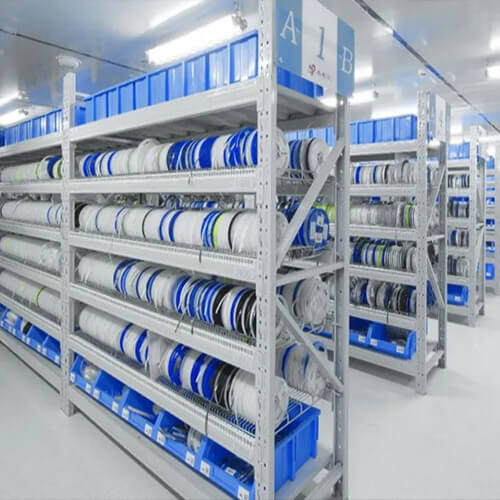
- Air-conditioned and static-free work environment
- Rigid, flex, and multi-layer PCB assembly
- Wide selection of materials
- Large scale PCB assembly
- Lead free and quick turn PCB assembly
Application of Consumer Electronics PCBs
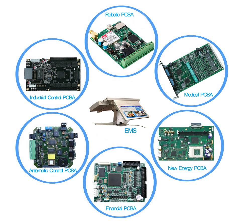
Consumer Electronics PCBs find extensive application in a wide range of products including but not limited to:
- Wearable devices
- Stereo players
- Camcorders
- LED and Retail Lighting
- Vending Machines
- Digital Camera Systems
- Video gaming consoles
- Wired and wireless mouse
- Computer monitors
- Televisions
- Printers and fax machines
- Smartphones
- Solid State Drives
- Computers
- Tablets
Consumer Electronics PCB
Frequent Questions
The consumer electronics PCB is applicable to mechanically support and electronically connect the electronics components using conductive tracks, pathways, signal traces and more.
The most advance trends of consumer PCB electronic products are miniaturization and diversification. There are many other trends as well including integrated circuits development, passive and discrete devices, substrate board, environmental protection awareness and more.
With miniaturization as a dominant trend for consumer electronics, PCBs are also continuously evolving. Rigid flex PCBs and HDI PCBs are some formats that are gaining popularity with portable electronics.
Yes, absolutely. We offer strong design for manufacturing services that ensure you get the best quality PCBs and you do not have to contend with costly errors.
Totally. Count on us to undertake electrical testing as also Flying Probe Testing to ensure efficacy.
You could get an instant quote on submitting your custom requirements. All you need to do is to request a quote for consumer electronics PCB and fill up the details. You could also write in to us at [email protected] or call us at +86 13823765993 for nay clarifications. We will be happy to hear from you and offer bespoke solutions.
Absolutely. Irrespective of the complexity of design or the number of layers, our teams are fully equipped to offer you reliable products.
Yes, the choice of finish is recommended basis the environment the PCB has to work in.
Totally. We understand the importance of quick turnaround times in competitive industries such as consumer electronics and are committed to the cause.
Yes, from prototypes to full production runs, we handle it all.
Rest assured, our prices are extremely cost-effective.

