Comprehensive Guide to RF PCB Design
The rise of high-tech electronic devices, from smartphones to IoT-enabled gadgets, has fueled the demand for Radio Frequency (RF) PCBs, which facilitate wireless communication by transmitting and receiving RF signals. While RF PCB design shares some similarities with traditional PCB design, it introduces unique complexities such as signal integrity, impedance matching, and high-frequency performance.
This article provides a comprehensive guide to RF PCB design, covering key concepts, design considerations, best practices, applications, and manufacturing/testing processes.
What is RF PCB?
RF PCB refers to a Radio Frequency Printed Circuit Board, operating within a frequency range of 100 MHz to 100 GHz. These specialized PCBs are integral to devices that rely on wireless communication for data transfer.
RF PCB design is inherently more complex than traditional PCB design, requiring careful attention to signal integrity, impedance matching, noise reduction, and thermal management.
Applications of RF PCBs
RF PCBs are central to numerous modern technologies, enabling seamless wireless communication. Common applications include:
- Communication Industry: Cellular networks, 5G devices, and satellite communications.
- Security Systems: Surveillance cameras and wireless alarms.
- Consumer Electronics: Smartphones, smartwatches, and Wi-Fi routers.
- Medical Applications: Remote patient monitoring and diagnostic equipment.
- Military Applications: Radar systems, secure communications, and drones.
- Automotive Industry: Vehicle-to-everything (V2X) communication and advanced driver-assistance systems (ADAS).
- Aerospace Industry: Navigation and communication systems for aircraft.
- Industrial Applications: IoT sensors and robotics.
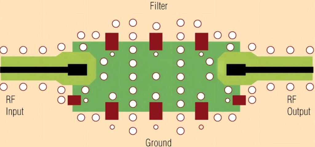
Key Considerations in RF PCB Design
Designing RF PCBs involves mitigating high-frequency challenges and ensuring optimal performance. Below are the primary considerations:
1. Impedance Matching
- Ensures efficient power transfer and minimizes signal reflection.
- Critical for maintaining signal integrity, especially between antennas and components.
2. Crosstalk Mitigation
- Higher frequencies increase the risk of signal interference between traces.
- Proper trace spacing and routing reduce data corruption.
3. Grounding and Shielding
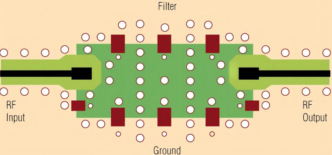
- Use dedicated ground planes to minimize electromagnetic interference (EMI).
- Incorporate shielding techniques to isolate high-frequency signals.
4. Component Selection and Placement
- Choose components with appropriate frequency ranges, noise-handling capabilities, and impedance characteristics.
- Place components strategically to minimize signal distortion and crosstalk.
5. Material Selection
- Opt for materials with low dielectric loss and a stable dielectric constant (e.g., Rogers, Taconic).
- Ensure thermal stability and minimal moisture absorption to enhance signal integrity.
6. Thermal Management
- Manage heat generated by active components like amplifiers using thermal vias, heat sinks, or thermal paste.
- Keep heat-sensitive components away from high-power zones.
7. Layer Stackup Design
- Utilize multi-layer stackups to separate signal, ground, and power layers.
- Ensure ground planes are close to signal layers to minimize signal return paths.
8. RF PCB Routing Best Practices
- Minimize trace lengths to reduce signal loss.
- Avoid parallel routing of RF and copper traces.
- Use curved or angled traces to prevent impedance mismatches.
RF PCB Manufacturing and Testing
1. Manufacturing RF PCBs
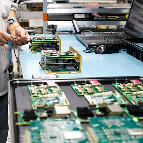
- Requires precision tools like laser drills and milling machines to achieve the tight tolerances needed for high-frequency circuits.
- Collaboration with experienced manufacturers ensures adherence to design specifications.
2. RF PCB Testing
Testing ensures that RF PCBs meet performance standards and operate reliably:
- Visual Inspection: Detects physical defects in PCBs.
- Electrical Connection Testing: Ensures proper connectivity across layers.
- Time Domain Reflectometer (TDR): Verifies impedance matching and signal integrity.
- Spectrum and Network Analyzers: Evaluate RF performance metrics.
Conclusion
RF PCB design is critical to enabling wireless communication and data transfer in modern electronics. With advancements in 5G and IoT technologies, the demand for RF PCBs has grown exponentially. However, designing and manufacturing RF PCBs requires specialized expertise to address challenges unique to high-frequency circuits, including signal integrity, crosstalk, and thermal management.
Partnering with experienced designers and manufacturers is essential to creating reliable RF PCBs that meet the demands of today’s technology-driven world.


