Comprehensive analysis of high-frequency boards definition, materials, design, process and signal transmission
1.1 Definition of high frequency board
High frequency board, also known as high frequency printed circuit board (High Frequency PCB), is a specially designed circuit board that can process and transmit high frequency signals. This kind of circuit board needs to consider many factors when designing and manufacturing to ensure the integrity and reliability of the signal during high-speed transmission. The following is the definition of high frequency board:
Frequency range: Generally speaking, high-frequency boards can be defined as PCBs with a frequency above 1GHz. They are mainly used in PCBs in the fields of high frequency (frequency greater than 300MHz or wavelength less than 1 meter) and microwave (frequency greater than 3GHz or wavelength less than 0.1 meter).
Material selection: High-frequency boards are usually made of specific materials, such as Rogers, Taconic, Isola, F4B (Teflon), TP-2, etc. These materials have high dielectric constants and low loss factors, and are suitable for applications in high-frequency communications and microwave fields.
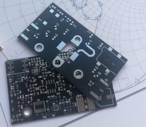
Performance characteristics: Due to the skin effect of high-frequency circuits, high-frequency boards need to have good dielectric properties to ensure effective transmission of high-frequency components and reduce signal attenuation. In addition, high-frequency boards also need to have high precision, high stability and good heat dissipation performance.
1.2 Application fields of high frequency boards
Communication equipment: wireless base stations, satellite communication equipment, antenna systems, filters, etc. require high-frequency boards to support high-speed data transmission and stable communication. Automotive electronics: in-vehicle entertainment systems, navigation systems, advanced driver assistance systems (ADAS), and automotive anti-collision radars, etc., use high-frequency boards to achieve complex electronic control functions. Medical equipment: diagnostic equipment and treatment equipment use high-frequency boards to transmit precise medical data and images. Aerospace and military fields: airborne and ground radar systems, millimeter wave applications, etc., use the high temperature resistance, corrosion resistance, and high insulation characteristics of high-frequency boards.
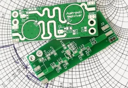
Consumer electronics: Smart homes, wearable devices, TVs, mobile phones, cameras, etc. use high-frequency boards to achieve faster data processing and transmission. Industrial control: Instruments, meters, industrial control automation communications, etc. require high-frequency boards to ensure the speed and stability of signal transmission. Radio frequency identification (RFID): High-frequency boards are used in tags and readers to achieve fast data reading and writing. Live broadcast satellite: High-frequency boards are used to process high-frequency signal transmission. Microwave links: Applications such as E-band point-to-point microwave links require low-loss high-frequency boards to reduce signal attenuation during transmission. Servers and data centers: With the development of cloud computing and big data, the demand for high-frequency boards used in servers and data centers is also growing.
2. Material characteristics of high frequency board
2.1 Dielectric constant and dielectric loss
2.1.1 Dielectric constant (Dk)
The dielectric constant is a physical quantity that describes the material’s ability to store charge in an electric field. For high-frequency boards, the size of the dielectric constant directly affects the signal transmission rate and quality.
Feature analysis:
Small and stable: The dielectric constant of the high-frequency board substrate must be small and stable. Generally speaking, the smaller the dielectric constant, the better. This is because the signal transmission rate is inversely proportional to the square root of the material’s dielectric constant, and a high dielectric constant can easily cause delays in signal transmission.
Frequency dependence: The dielectric constant may change with frequency. For example, the dielectric constant of Rogers RO4350B high-frequency board is measured at 10GHz with a value of 3.48, while at 24GHz, the dielectric constant drops slightly to 3.47.
Material selection: In order to meet the transmission requirements of high-frequency signals, high-frequency board materials usually use materials with low dielectric constants, such as polytetrafluoroethylene (PTFE) thermoplastic materials and hydrocarbon resin (PCH) thermosetting materials.
2.1.2 Dielectric loss (Df)
Dielectric loss refers to the energy loss caused by various mechanisms inside the material (such as polarization, conductivity, etc.) under the action of the electric field. For high-frequency boards, the size of the dielectric loss directly affects the quality of signal transmission.
Feature analysis:
Must be small: The dielectric loss of high-frequency panels must be small. The smaller the dielectric loss, the smaller the signal loss during transmission, thus ensuring the quality of signal transmission.
Influencing factors: Dielectric loss is affected by many factors, including the dielectric constant, conductivity, frequency, etc. For example, at 24GHz, the loss tangent of the green oil dielectric in the Rogers RO4350B high-frequency board is large, which will further increase the insertion loss of the microstrip line.
Material selection: In order to reduce dielectric loss, high-frequency board materials usually use materials with low dielectric loss characteristics, and further reduce losses by optimizing material formulation and manufacturing process.
2.2 Electrical and thermal conductivity
2.2.1 Electrical conductivity
Conductive material: High-frequency boards usually use copper foil as the conductive layer. The thickness and surface roughness of the copper foil will affect its conductive properties. The smoother the copper foil, the lower the resistance and the better the conductive properties.
Skin effect: In high-frequency signal transmission, due to the skin effect, the current tends to flow on the surface of the conductor, which requires the high-frequency board to use low-profile copper foil to reduce transmission loss.
Surface treatment: The surface treatment technology of high-frequency boards, such as chemical gold plating (ENIG), chemical silver plating, organic solderability protection film (OSP), etc., will also affect its conductive properties.
2.2.2 Thermal conductivity
Thermally conductive material: The substrate material of the high-frequency board should have good thermal conductivity to help dissipate heat and maintain stable operation of the circuit. Some special high-frequency board materials, such as Rogers’ PTFE (polytetrafluoroethylene) substrate, have high thermal conductivity.
Coefficient of thermal expansion (CTE): The coefficient of thermal expansion of the high-frequency board should be close to that of the copper foil to reduce thermal stress and improve circuit reliability.
Thermal management: Thermal management strategies must be considered when designing high-frequency boards, such as using thermally conductive materials, heat dissipation channels, thermal interface materials, etc. to improve thermal conductivity.
2.3 Effect of material selection on high-frequency performance
2.3.1 Common high-frequency board materials include:
Polytetrafluoroethylene (PTFE) substrate: has extremely low dielectric constant and dielectric loss factor, suitable for high-frequency applications.
Modified polyphenylene ether (PPO) substrate: Improve electrical properties and processing performance through modification.
Cyanate resin substrate: has excellent electrical insulation properties and high temperature resistance.
Epoxy resin substrate: lower cost, but relatively poor dielectric properties.
2.3.2 The selection of high-frequency board materials has a significant impact on high-frequency performance, mainly involving the following aspects:
1. Dielectric constant (Dk):
The dielectric constant is a measure of a material’s ability to store energy in an electric field, which has a direct impact on the speed at which signals are transmitted. A low dielectric constant helps reduce signal propagation delays and increase transmission speeds.
2. Dielectric loss factor (Df or tan δ):
The dielectric loss factor reflects the degree of energy loss of a material in an AC electric field. A low dielectric loss factor can reduce signal attenuation during transmission and improve signal transmission quality.
3. Coefficient of Thermal Expansion (CTE):
The thermal expansion coefficient of the high-frequency board should be close to that of the copper foil to reduce thermal stress and improve dimensional stability.
4. Heat resistance (Tg):
High-frequency boards work in high-temperature environments, so they need to have a high glass transition temperature (Tg) to maintain stable performance.
5. Mechanical properties of materials:
High frequency board materials should have good mechanical properties, such as tensile strength and impact resistance, to ensure reliability during manufacturing and use.
6. Material processing properties:
High-frequency board materials should be easy to process, including drilling, lamination, pattern transfer and other processes.
7. Cost-effectiveness:
The selection of materials also needs to consider cost factors to meet the economic requirements in different application scenarios.
8. Environmental adaptability:
High frequency board materials should have good chemical stability and weather resistance to adapt to different usage environments.
3. High-frequency board design principles
3.1 Signal Integrity Design
In high-frequency board design, signal integrity (SI) is one of the key factors to ensure the normal operation of electronic equipment. Signal integrity design mainly focuses on how to reduce signal distortion and loss during transmission. The following are some basic signal integrity design principles, especially the key points about impedance control:
3.1.1 Impedance Control
Consistency: Ensure that the impedance of the entire signal path remains consistent to avoid signal reflections caused by impedance mutations.
Calculation: Accurately calculate the characteristic impedance of transmission lines, including microstrip and stripline.
Matching: Impedance matching is performed at the source and load ends, using terminal matching techniques such as series or parallel matching.
Differential impedance: For a differential signal pair, keep the impedance of the two signal lines balanced.
3.1.2 Transmission Line Design
Trace width: Determine the trace width based on the required characteristic impedance and maintain consistency.
Trace spacing: For differential signals, maintain constant spacing to maintain consistent differential impedance.
Trace length: Try to shorten the trace length to reduce signal transmission delay and attenuation.
Trace shape: Avoid sharp angles and right angles, use arcs or 45-degree angles to reduce impedance discontinuity.
Reference plane: Ensure that the transmission line has a stable reference plane to maintain signal integrity and impedance control.
Via design: Design vias reasonably to reduce the impact on impedance continuity and signal transmission performance.
Blind buried via technology: Blind buried via technology is used in multilayer boards to provide better signal connection and shorter transmission path.
Electromagnetic compatibility (EMC): Consider EMC when designing transmission lines to reduce crosstalk and radiation.
Layout of signal layers and ground layers: Reasonably layout the signal layers and ground layers to provide a good signal loop and reduce noise.
Material selection: Choose PCB materials suitable for high-frequency applications, with low dielectric constant and low dielectric loss factor.
Thermal Effects: Evaluate thermal effects on high-frequency signal transmission to ensure impedance control is not significantly affected by temperature changes.
Test and simulation: Use high-frequency transmission line simulation tools to predict and test before design to ensure that the design meets performance requirements
3.2.1 Shielding technology
Shielding materials: Select appropriate shielding materials, such as copper foil, aluminum foil or special shielding coatings to provide good electromagnetic shielding effect.
Shield integrity: Ensure the integrity of the shielding layer to avoid cracks or openings, which may be paths for electromagnetic leakage.
Seam treatment: Take appropriate overlapping or sealing measures at the seams of the shielding body to maintain the continuity of the shielding.
Shield grounding: Properly ground the shield to provide a low-impedance return path to reduce electromagnetic interference.
Multilayer board shielding: In multilayer board design, internal ground layers are used as shielding to reduce the effects of external electromagnetic fields.
Signal line shielding: For particularly sensitive signal lines, consider using partial shielding or shielded cable.
3.2.2 Grounding strategy
Single-point grounding: For low-frequency signals, single-point grounding can reduce the ground loop area and ground impedance.
Multi-point grounding: For high-frequency signals, multi-point grounding helps reduce ground impedance and provide a better signal return path.
Hybrid grounding: In complex systems, it may be necessary to combine single-point grounding and multi-point grounding strategies.
Ground plane: In PCB design, provide a continuous ground plane to serve as a return path for signals and reduce electromagnetic radiation.
Layer segmentation: In multi-layer board design, the layer should be segmented reasonably to control noise and improve signal integrity.
Ground vias: Use vias to connect different ground layers to ensure good vertical conductivity.
Decoupling capacitors: Place decoupling capacitors near power supplies and critical signals to provide a local, low-impedance path to ground.
Ground path: Optimize the ground path and reduce the loop area to reduce electromagnetic radiation and improve anti-interference capabilities.
Signal integrity and grounding: Consider the relationship between signal integrity and grounding during design to ensure that high-speed signals have a suitable grounding strategy.
3.3.1 Heat conduction path
Material selection: Choose materials with high thermal conductivity, such as copper, aluminum, or specific metal substrates to improve heat conduction efficiency.
Layout optimization: Reasonably arrange heat sources, such as power devices and high-frequency amplifiers, to reduce the distance that heat is conducted inside the PCB.
Thermal vias: Use thermal vias to conduct heat from the heat source to the other side or edge of the PCB for easy heat dissipation.
Thermal Interface: Use thermal pads or thermally conductive adhesives to transfer heat from the device to the PCB or heat sink.
Coefficient of thermal expansion: Consider the thermal expansion coefficient of the material to ensure the dimensional stability of the PCB under temperature changes.
3.3.2 Heat dissipation design
Heat sink: Design heat sinks for high power devices to increase the heat dissipation area and improve the efficiency of natural or forced convection.
Fans and Cooling Systems: Use fans or liquid cooling systems to enhance heat dissipation when necessary.
Thermal Isolation: Design thermal isolation zones around heat sources to reduce the impact of heat on surrounding sensitive areas.
PCB thickness: Increase the thickness of the PCB appropriately to provide a larger heat conduction path.
Embedded devices: Consider using embedded device technology to embed devices inside the PCB to improve heat conduction efficiency.
Thermal Simulation: Perform thermal simulation analysis to predict heat distribution and hot spots under different operating conditions.
Temperature monitoring: Design temperature monitoring points, such as using thermistors or thermocouples, to monitor the temperature status of the equipment in real time.
Natural convection: Optimize the shape of the housing and PCB to promote natural convection and improve heat dissipation efficiency.
Forced convection: In situations of high heat loads, use forced convection (such as fans) to assist in cooling.
Thermal Cycle Test: Thermal cycle test is performed to evaluate thermal stability and reliability under long-term operation.
4. High Frequency Board Manufacturing Process
4.1 Substrate Manufacturing Technology
Material selection: Choose materials suitable for high-frequency applications, such as Rogers, Taconic, Isola, F4B (Teflon), TP-2, etc. These materials have different dielectric constants and dielectric loss factors.
Lamination process: Use lamination technology to combine different material layers (such as copper foil, dielectric layer and reinforcement material) to form a multi-layer structure.
Copper foil attachment: Copper foil is attached to the dielectric layer. Copper foil serves as a conductive layer, and its thickness and surface roughness will affect signal transmission.
Hole processing: Form through holes, blind holes or buried holes on the substrate by mechanical drilling or laser drilling to achieve electrical connection between different layers.
Surface treatment: The substrate surface may require special treatment, such as immersion gold, tin spraying, gold plating, silver plating or organic solderability (OSP) treatment to improve soldering performance and anti-oxidation ability.
4.2 Conductor manufacturing technology
Conductor Fabrication: Fine conductors are fabricated on the substrate, these can be etched copper or using other conductive materials.
Impedance control: Precisely control the wire width and spacing to achieve the required characteristic impedance.
Surface plating: A wear-resistant and corrosion-resistant metal layer, such as nickel, gold or tin, is plated on the surface of the conductor to improve the durability and reliability of the conductor.
Plating process: Use electroplating technology to fill the guide holes to ensure good electrical connection and mechanical support.
Pattern transfer: Transferring the conductor pattern from the mask to the substrate, usually using photoresist and exposure equipment.
4.3 High frequency characteristics test method
Impedance testing: Measures the characteristic impedance of a transmission line to ensure it meets design specifications.
Transmission loss test: Evaluates the loss of a signal during transmission, usually at high frequencies.
Electromagnetic compatibility test: Test the electromagnetic interference (EMI) and electromagnetic susceptibility (EMS) of high-frequency boards to ensure that they meet electromagnetic compatibility requirements.
Signal integrity testing: Evaluate the integrity of the signal using a time domain reflectometer (TDR) or frequency domain analyzer.
Thermal Performance Testing: Evaluate the thermal conductivity and thermal expansion coefficient of high-frequency boards to predict their thermal behavior under actual operating conditions.
Reliability test: Accelerated aging test and environmental adaptability test are performed to evaluate the long-term reliability of high-frequency boards.
5. Signal transmission technology of high frequency board
5.1 Microstrip and Stripline
Microstrip line: is a conductive strip on the surface of a dielectric substrate, usually parallel to the ground plane. It is suitable for microwave frequencies because they provide low loss and controlled characteristic impedance.
Stripline: Unlike microstrip, stripline is a conductive strip embedded inside a dielectric substrate with ground planes on both sides. Stripline provides better shielding at high frequencies and reduces electromagnetic interference.
5.2 Waveguide and Slotline
Waveguide: A metal tube used to transmit microwave signals, which reduces losses by confining electromagnetic waves to propagate in a specific mode. Waveguides are commonly used in high-performance radio frequency systems such as radar and communications equipment.
Slotted line: A transmission line with slots engraved on the surface or inside of a dielectric substrate. It transmits signals by propagating electromagnetic waves in the slots. Slotted lines can provide good shielding effects and are suitable for high-density circuit design.

5.3 Differential Signal Transmission
Differential signaling: A transmission method that uses two signal lines with equal potential but opposite polarity. Differential signaling is very effective in reducing electromagnetic interference and improving signal integrity.
Differential pairs: In high-frequency board design, differential signals are usually implemented through differential pairs, which requires that the length, width, and spacing of the two signal lines be strictly consistent to ensure impedance matching and signal synchronization.
{High-frequency board_high-frequency PCB board_RF board proofing_2-20 layer circuit board manufacturer-Xinchenger Electronics} is a powerful manufacturer mainly engaged in 2-20 layers of high-frequency microwave radio frequency induction printed circuit board quick samples and small and medium batches. Specializing in the production of high-frequency, high-precision, high-density environmentally friendly PCB circuit boards. The main products are: high-frequency PCB circuit boards, Rogers/Rogers high-frequency boards, Taconic/Taconic high-frequency boards, F4B/Teflon high-frequency boards, microwave radio frequency boards, special circuit boards, etc. We have rich production experience in high-frequency circuit boards used in data communications, wireless communication base stations, radar systems, automobiles, medical, military and other industries.
As a leading PCB manufacturer, members of our printed circuit board (PCB) design service team are practical partners working with you on every project and can help you achieve your goals at any time. They can complement your engineering expertise, which helps speed up time to market, reduce the time from concept to production, and ensure that quality is integrated into the manufacturing process to maximize your profits.


