


Common PCB Tolerances for Manufacturing
PCB tolerances for manufacturing refer to the allowable variations from specified dimensions, encompassing:
- material thickness,
- copper thickness,
- drilling, plating,
- and solder masks.
These PCB tolerances ensure that PCB circuit boards are produced precisely and can function as intended. Manufacturers adhere to specific in-house tolerance guidelines, based on international standards like IPC-A-600 Class 2, to maintain quality throughout the production process.
While tighter tolerances can increase costs and extend lead times, they are sometimes necessary, especially for advanced designs like High-Density Interconnect (HDI) or Micro Fineline Technology (MFT) boards.
Standard Tolerances
As a whole, PCB tolerances are almost completely a function of your PCB manufacturer’s capability. For this reason, discussing specific absolute tolerances is not possible. In this article, we’ll discuss typical PCB tolerances you might encounter, common for many manufacturers.
- Copper to Edge of PCB Tolerance: For outer layers, a minimum of 0.010″ is common, while inner layers should have a minimum of 0.015″ (with a preferred 0.020″ for inner layers). When scoring, the minimum requirement is 0.015″ for outer layers and 0.020″ for inner layers.
- Pad Size and Annular Rings: Regarding pad size and annular rings, the pad should be at least 0.010″ larger than the finished hole size for vias and 0.014″ larger for component holes. Consequently, the annular ring (the radius of the pad) must be at least 0.005″ for vias and a minimum of 0.007″ for component holes.
Bow and Twist
Bow and twist PCB tolerances refer to the flatness criteria for assessing potential alignment issues in a circuit board.
- Bow is the curvature deviation from flatness, forming a cylindrical or spherical curve on a rectangular plane.
- Twist occurs when one corner of a rectangular circuit board is lifted out of the plane formed by the other three corners, causing a deformation.
For non-rectangular boards, bow and twist can be evaluated by overlaying a rectangle on the PCB during testing to measure the deviation.
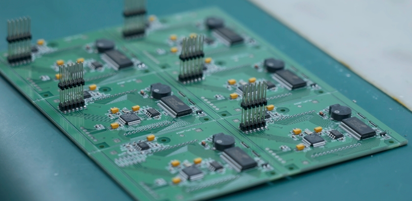
PCB with a variety of different traces, holes, and required tolerances.
Common Hole Size Tolerances
Hole tolerances are particularly important for the placement of through-hole components and vias. These tolerances determine the accuracy of hole diameters and their placement on the board. Tooling tolerances are influenced by factors such as drill bit wear, the type of drilling equipment used, and the board material’s properties. Inaccurate hole drilling can lead to component misalignment or failure in establishing reliable electrical connections.
- For plated through-holes (PTH), holes with a diameter of 0.8mm or less have a tolerance of ±0.08mm, while holes between 0.8mm and 2.5mm are held to a tolerance of ±0.1mm.
- Larger PTHs, ranging from 2.5mm to 6.3mm, have a tolerance of ±0.15mm, and any hole greater than 6.3mm carries a tolerance of ±0.2mm.
- Non-plated through-holes (NPTH) are generally held to a tighter tolerance, with holes up to 6.3mm having a tolerance of ±0.05mm, and those larger than 6.3mm adhering to specific manufacturer guidelines.
- For holes up to 0.250″ in diameter, a standard tolerance of +/- 0.005″ is typically applied, with larger holes subject to routing tolerances, especially when dealing with different copper weights in PCB construction.
Circuit Board Thickness
Thickness tolerance pertains to the overall thickness of the PCB and the individual layers within multilayer boards. This tolerance is important not only for fitting the board within its enclosure but also for ensuring it can withstand the physical and thermal stresses it will encounter in operation. Thickness tolerances affect aspects such as the board’s stiffness, its thermal management properties, and its ability to support heavy components. Like other tolerances, thickness tolerance varies depending on the materials used and the manufacturing technology.
- Standard PCB thicknesses typically include 31 mils, 62 mils, 93 mils, and 125 mils.
- For boards with a thickness of 31 mils and above, the tolerance is ± 10%.
- For boards thinner than 31 mils, the tolerance is ± 0.003″.
- Generally, thickness tolerances may vary by 10%, with a minimum of +/- 0.005″.
Regarding minimum board thickness, the default requirements are as follows:
- 2-layer boards: The standard thickness is .020″.
- 4-layer boards: The standard thickness is .020″.
- 6-layer boards: The standard thickness is .031″.
- 8-layer boards: The standard thickness is .047″.
- 10-layer boards: The standard thickness is .062″.
Copper Trace Width Spacing
Copper spacing refers to the minimum distance between any two adjacent copper features on a PCB, while trace width is the minimum width of a copper feature, typically the traces. The required trace width and spacing depend on the thickness of the copper used:
- For 1 oz. finished copper weight on inner layers, the minimum trace width and spacing is 0.003″.
- For 2 oz. finished copper weight on both inner and outer layers, the minimum trace width and spacing is 0.005″.
- For 3 oz. finished copper weight on both inner and outer layers, the minimum trace width and spacing is 0.009″.
- For 4 oz. finished copper weight on both inner and outer layers, the minimum trace width and spacing is 0.010″.
Drilling Tolerances
The drilling process creates vias and establishes interconnections between layers in a PCB. A design engineer must review the board manufacturer’s capabilities and tolerances before placing an order to ensure the design can be accurately fabricated.
Key drilling features and their tolerances include:
- Drill diameter tolerance for both PTH and NPTH drills is ±3 mils (0.003″).
- The minimum spacing between a drilled hole and adjacent copper features (drill to copper) is 8 mils (0.008″).
- Tolerance for the location or registration of drilled holes is 1 mil (0.001″).
- The minimum spacing between two drilled holes (drill to drill) is 6 mils (0.006″).
- The minimum distance between a drilled hole and the board edge (drill to board edge) is 6 mils (0.006″).
- Annular ring tolerances are specified by the designer.
- Tolerances for laser hole location are set at 5 mils (0.005″).
Routing Tolerances
When designing and manufacturing PCBs, precise drilling ensures reliable connections and board functionality. The following tolerances are key considerations in the drilling process:
- The tolerance for drill diameters, both for PTH (Plated Through-Hole) and NPTH (Non-Plated Through-Hole) drills, is ±3 mils (0.003”).
- The minimum spacing between a drilled hole and adjacent copper features (drill to copper) must be at least 8 mils (0.008”).
- The tolerance for the precise location or registration of a drilled hole is 1 mil (0.001”).
- The minimum allowable distance between two drilled holes (drill to drill) is 6 mils (0.006”).
- The minimum spacing between a drilled hole and the edge of the board (drill to board edge) is 6 mils (0.006”).
- Annular ring tolerances are determined by the designer based on the specific requirements of the board.
- The tolerance for placing laser-drilled holes is set at 5 mils (0.005”).
Controlled Impedances
When designing PCBs with controlled impedance, maintaining precise tolerances is crucial to ensure signal integrity. The standard tolerance for controlled impedance is set at 10%. For more advanced designs, this tolerance is tightened to 5%, and for micro designs, the tolerance also remains at 5% to meet the stringent requirements of high-performance applications.
KKPCB is a professional manufacturer dedicated to providing high-quality, zero-defect PCB and PCBA solutions. We specialize in offering comprehensive one-stop electronic manufacturing services, including PCB design, PCB manufacturing, component sourcing, SMT assembly, and DIP soldering.