Common Challenges and Solutions in SMT Board Assembly
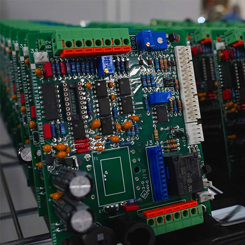
Surface Mount Technology (SMT) board assembly is a critical and widely used process in modern PCB manufacturing. This process involves placing and soldering electronic components directly onto the surface of PCB pads. Alongside Plated Through-Hole (PTH) assembly, it is one of the two primary PCB assembly methods.
SMT assembly is highly efficient and accurate, making it ideal for complex and high-density PCB designs. However, its intricate processes and the use of small-sized components present unique challenges for manufacturers. This article outlines the most common challenges in SMT board assembly and provides actionable solutions to address them.
What is SMT Board Assembly?
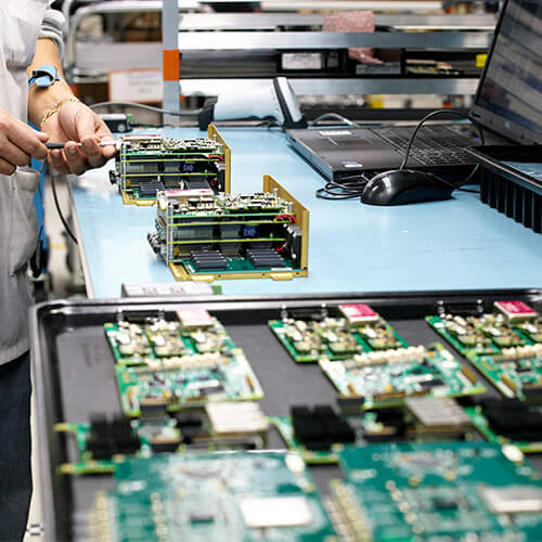
SMT board assembly refers to the automated process of assembling electronic parts onto PCBs using Surface Mount Technology. It ensures precision and efficiency but requires attention to detail due to the small size of components and the need for adherence to strict design and assembly protocols.
Common Challenges and Solutions in SMT Board Assembly
Below are some frequent challenges faced during the SMT board assembly process and their respective solutions:
1. Rework
Rework involves repairing or replacing faulty parts identified during quality inspection. It is challenging due to the precision required in removing and repositioning components.
Solution:
- Ensure accurate placement of components during the initial assembly process.
- Verify the SMT assembly capability and alignment during the design phase.

2. Improper Soldering
Bad solder joints result from insufficient solder paste application or inadequate pad size. These can cause electrical connection failures.
Solution:
- Apply solder paste in the early stages of SPI (Solder Paste Inspection) or DFA (Design for Assembly).
- Adhere to IPC standards for pad aspect ratio to ensure sufficient solder paste application.
3. Testability
Dense component placement around test points makes it difficult to conduct quality checks using flying probes.
Solution:
- Place SMT components to allow easy access to test points.
- Collaborate with designers to adjust test point positions as needed.
4. Solder Bridges
Solder bridges occur due to excessive solder application, improper stencil design, or reflow profile issues, causing short circuits between component pins.
Solution:
- Design accurate solder masks and follow IPC standards for pad size and stencil data.
- Use fiducials and control the reflow profile to minimize solder bridges.
5. Solder Ball Joints
Solder balls often result from misaligned stencils, moisture issues, or improper reflow profiles, affecting the quality of connections.
Solution:
- Check and align the solder stencil before assembly.
- Monitor the reflow profile and implement moisture protection measures.
6. Wrong Parts
Misalignment or incorrect placement of parts can occur due to errors in the pick-and-place process or mismatched silkscreen polarity.
Solution:
- Ensure alignment in the DFA stage and double-check polarity markings.
7. Tombstoning
This defect occurs when one side of a component lifts vertically during reflow soldering, commonly affecting small components like MLCCs.
Solution:
- Improve pad size and placement consistency.
- Conduct quality inspections before reflow soldering.
8. Cold Joints
Cold solder joints, caused by incomplete melting during reflow, result in weak connections and impurities.
Solution:
- Use proper soldering techniques and monitor parameters such as temperature, density, and reflow speed.
9. Signal and Power Integrity
Improper component placement or design can reduce signal and power integrity, leading to degraded PCB performance.
Solution:
- Ensure isolation and proper placement of bypass capacitors near power pins to reduce noise.
- Use precise schematic designs to enhance signal integration.
10. Shadowing
Excessive solder on small components during wave soldering can cause shadowing defects.
Solution:
- Utilize an accurate solder template and modify PCB pad designs to match component sizes.
Conclusion
Understanding and addressing the common challenges in SMT board assembly is crucial to ensuring efficient and reliable PCB production. Following SMT assembly standards, IPC design rules, and implementing the suggested solutions can significantly reduce defects and improve manufacturing outcomes. By prioritizing precision in design and assembly processes, manufacturers can overcome these challenges and deliver high-quality PCBs.


