Flexible PCB: How to Choose the Right Assembly Technology
What is a flexible PCB?
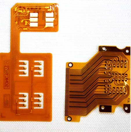
Flexible PCB is a unique type of printed circuit board that replaces the rigid FR4/metal/PTFE/ceramic substrate with a thin, bendable polyimide (PI) substrate and replaces the solder mask with a PI coverlay. Plated through holes or buried vias insulate and protect the conductive copper traces that connect the various flexible PCB layers to the non-conductive PI material. Flexible circuit board, flexible PCB or FPC is another name for flexible PCB.
The non-conductive flexible polyimide material is etched with copper circuit traces, and plated through holes (PTH) or buried vias connect the various circuit layers. Electronic components can be surface mounted on PCB pads on both sides of the flexible PCB. Flexible PCBs sometimes have PCB stiffeners added to the ends for connection to systems, devices or other parts to provide better mechanical support.
Flexible PCBs can be single-sided, double-sided, single-layer, dual-layer or multi-layer, and can also be custom designed and manufactured. One PCB layer equals one circuit layer. But everyone can quickly distinguish between flexible PCBs and standard rigid PCBs because they are usually thin, light and yellow. Its thickness ranges from 0.05mm to 0.6mm. This is also the complete flexible PCB thickness range of PCBONLINE. Usually, flexible PCBs have two sides. To understand them correctly, you must be familiar with the basic structure of flexible PCBs.
Difference between Polyimide (PI) and Polyester (PET) Materials
Flexible PCB raw materials and stacking determine the quality of flexible circuits. According to market demand, three different types of basic raw materials are used to manufacture flexible circuit boards. Polyester (PET), polyimide (PI) with adhesive, and polyimide (PI) without adhesive. The advantages of PET materials include simpler production methods, lower costs, and shorter delivery times. The disadvantages of PET materials include that polyester cannot pass soldering flows.
Therefore, it cannot work in hot climates. The advantage of polyimide (PI) is that it is flexible. It can work in hot environments. The cost of raw materials is significantly higher than that of polyimide (PI), which is one of its disadvantages.
Why must flexible PCBs be unique and not just make every PCB flexible?
Despite the usefulness of flexible circuit boards, rigid circuit boards are still necessary for some applications. The biggest barrier to using fully flexible circuit board designs in consumer products is cost effectiveness. Rigid circuit boards are less expensive to produce and install in a typical automated high-volume manufacturing plant. To reduce manufacturing and assembly costs, the best solution for innovative products is often to use wooden PCB circuit boards whenever possible and use flexible circuits only when necessary.
Some manufacturers even use hybrid rigid-flex printed circuit boards for this purpose. Laptops and medical devices that connect rigid circuit boards often use flexible circuits similar to ribbons. By focusing on the unique features of each circuit board base technology, these boards are combined and created to meet a wide range of technical needs.
Types of Flexible PCBs
Depending on the number of circuit layers, FPCs can be divided into single-layer, double-layer, and multi-layer.
FPCs are available in single-sided and double-sided versions, which differ depending on the side on which the components are mounted.
There are three types of flexible PCBs: transparent flexible PCBs, flexible aluminum PCBs, and yellow polyimide PCBs.
There are HDI and standard flexible PCBs for flexible PCBs, which differ in terms of FPC vias.
How to Choose the Right Assembly Technology for Flexible PCBs?
You can ensure that the flexible PCB you design or use is designed correctly by:
Choosing the Right Material for Your PCB
The process of manufacturing flexible PCBs starts with choosing the right materials. We mean choosing the right substrate material, conductors, adhesives, and coverlays. It will help if you consider using a film with solid insulation properties as the main material. It must be tested for mechanical and electrical properties as per standards.
For this reason, producers usually choose polyester or polyimide. FR4 is used for standard boards, but its thin variants can also be used, especially in flexible rigid boards.
When comparing different materials, polyester has the lowest solderable temperature. The lowest maximum continuous operating temperature is 110C, which is lower than FR4’s 150C and polyimide’s 220C. When it comes to absorbing moisture, polyimide is preferred due to its excellent tensile strength and elongation. The dielectric loss factor of polyimide is half that of polyester.
Overall, polyimide is a non-flammable material with excellent electrical and physical properties. Polyester, on the other hand, is less expensive and performs well enough, but is susceptible to damage during soldering.
Fabrication – Punching and Drilling: Key to Assembling PCBs
Material preparation is the first step in the assembly process. You should list all the supplies you will need for the process, also known as “punching”. This also includes laminating paste, separation film, and other auxiliary materials required. It can be difficult to handle thin and fragile materials during the drilling process. Experts recommend stacking the boards first because drilling is difficult. For example, think of a cladding and stacking all its components. After combining them, they may look like books, but they are thicker when combined than when they are alone.
Assembly Techniques – Pitting and Desmearing
If the drilling process is successful, there may be some residual drilling debris on the material. Therefore, you should try to remove all the dirt before moving on to the next step. However, this requires great vigilance because you are dealing with small and thin components. PTH (plated through hole) and pattern plating are the next steps in the process. Here is an example of the process:
- For electroless plating, experts recommend using acid colloidal palladium as a pre-treatment solution. They predict it will be more effective than alkaline ion palladium. The reason is that you don’t want the material to swell or create unnecessary holes. Also, focus on speed and reaction time as fast as possible.
- Electroplating: The electroless copper layer has poor mechanical properties, including flexibility. This makes it susceptible to thermal shock damage. The purpose of electroplating is to thicken the panel, because doing so ensures the integrity of the hole wall coating in subsequent processes.
- Imaging – Before entering this stage, clean the surface of the board. For standard PCBs, assemblers use similar techniques. However, since flexible boards can deform, it is helpful to use electrolytic and chemical cleaning methods. Now apply the dry film and watch it develop. Due to polymerization, it will become brittle and lose some of its copper foil bonding.
Etching
Etching is the next assembly technology we adopt. At the bending point, you will see many parallel wires on the substrate. If you want to maximize the etching effect, be careful to maintain the direction of the etching solution throughout the process. Also consider the transfer direction, pressure, and position. The rigid substrate will be connected to the flexible substrate. You need to pull the flexible substrate forward, so do it in front of it. After the etching process is completed, you need to modify the surface to increase the bonding potential. Then place the cladding. Also, make sure to bake the flexible board and cladding, as they have different potentials to absorb moisture. Bake for about 34 days, but make sure the stack height is a maximum of 25 mm.
Laminating PCBs
It is crucial to understand that the process details must be selected according to the selected substrate. The material will determine the time, pressure, and heating rate required for lamination. Some general tips to consider are as follows:
Ramp rate: The temperature should reach 173C within 10 to 20 minutes.
Use a pressure of 150N to 300N/cm2. It takes five to eight seconds to reach the maximum pressure.
Time – According to experts, the net pressure time will last about 60 minutes at maximum pressure.
For any complex use and professional applications, you need professional lamination equipment. Also, make sure to choose the right gasket material. Consider low flow and excellent formability, and choose a material that will not shrink after cooling.
Complete PCB Assembly
Baking, hot melting, and sharpening make up the final steps of the flexible PCB assembly process. Professionals use these techniques to remove excess moisture, dry them out, and protect the boards from moisture. Lastly, it would be beneficial if you consider packaging. Since wrapping paper alone cannot separate the boards, manufacturers use vacuum packaging techniques to pack large quantities of boards. The most trustworthy businesses will take every precaution to package the PCBs safely and ship them with a reliable service.
KKPCB conducts research on special processing technologies such as ordinary double-sided boards, thick copper circuit boards, high-frequency circuit boards, HDI circuit boards, rigid-flexible circuit boards, FPC flexible boards, buried blind hole circuit boards, and IC carrier boards. Provides PCB design, PCB layout, PCB prototyping and PCB assembly services.

