


Chip Scale Package Basics
Chip-Scale Package (CSP) is a type of integrated circuit packaging technology. The size of the package is up to 1.2 times the size of the actual die, with only a single-die and a direct surface mountable package. First originating in the 1990s, it was developed as a response to the demand for smaller and more efficient packages.
Types of Chip Scale Packaging
| Type | Applications | Advantages |
| Customized Leadframe-Based CSP (LFCSP) | Power management chips Applications needing thermal and electrical efficiency | Excellent thermal and electrical performanceAdaptable to various chip sizes and configurations |
| Flexible Substrate-Based CSP | Wearable devicesFlexible electronics | Resilient against mechanical stressVersatile for different shapes and innovative designs |
| Flip-Chip CSP (FCCSP) | CPUsGPUsHigh-performance computingGaming devices | Shorter signal path for faster data transferEfficient space utilization |
| Rigid Substrate-Based CSP (like FR4 or ceramic) | Automotive electronicsIndustrial applications | Robust physical supportGood heat dissipationReliable in harsh conditions |
| Wafer-Level Redistribution CSP (WL-CSP) | SmartphonesPortable devices | Extremely compact packagingCost-effective for high-volume production |
Technical Chip Scale Package Information
The defining characteristic of a chip scale package is that its size closely approximates that of the chip itself. Ideally, the smallest possible package is the size of the chip itself. Another important characteristic is the ball pitch, which is typically no more than 1 millimeter. The ball pitch refers to the distance between the centers of adjacent solder balls (or bumps) that connect the package to the motherboard or circuit board.
CSP Design
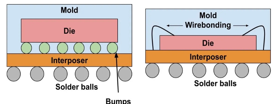
CSPs can be designed in different ways. One common approach involves mounting the die on an interposer, which is the small interface that bridges the connection between the die and the external contacts. On this interposer, pads or balls are formed, akin to what is seen in Flip Chip Ball Grid Array (BGA) packaging. Another approach is to create pads directly on the silicon wafer, bypassing the need for an additional interposer. This method results in a package that is very close to the size of the silicon die and is known as a wafer-level package (WLP) or wafer-level chip-scale package (WL-CSP). WLP or WL-CSP is particularly advantageous in terms of size reduction, as it eliminates additional layers between the silicon die and its external connections.
| Chip Scale Package Manufacturing Process | ||
| Step | Process | |
| 1 | The die is affixed to the interposer with epoxy. In scenarios where the die’s backside requires a connection to the circuit, such as in flip-chip packaging, conductive epoxy is employed | |
| 2 | The die is connected to the interposer through a process known as wire bonding, which is done using either gold or aluminum wires. These wires are strategically placed as low and as near to the die as feasible to keep the overall size of the package to a minimum | |
| 3 | The die and wires are encased in plastic | |
| 4 | Solder balls are affixed to the underside of the interposer | |
| 5 | The package is labeled and the individual parts are cut from the lead frame | |
Commonly Used Chip Scale Package Types
- Fine-Pitch Ball Grid Array (FPBGA) is characterized by its fine pitch and ball grid array, allowing for high density of I/O connections and commonly used in memory chips.
- Wafer-Level Chip-Scale Package (WLCSP) is a packaging process that occurs at the wafer level and is commonly used in mobile devices due to its compact size.
- Quad Flat No-leads Package (QNFP) features a small size and low profile. These types of packages have no leads and use a pad for electrical and thermal connections. This type is often found in automotive and consumer electronics.
KKPCB is a professional manufacturer dedicated to providing high-quality, zero-defect PCB and PCBA solutions. We specialize in offering comprehensive one-stop electronic manufacturing services, including PCB design, PCB manufacturing, component sourcing, SMT assembly, and DIP soldering.