Ceramic Substrates
- Home
- Ceramic Substrates
PCB Manufacturing
and PCB Assembly
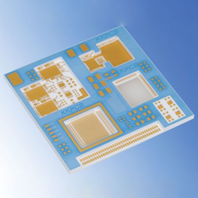
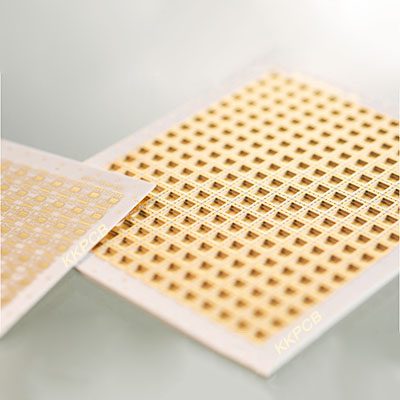
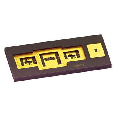
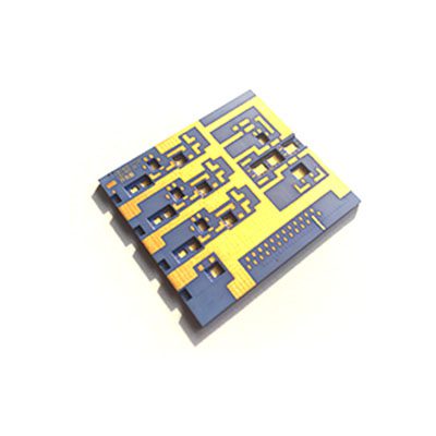
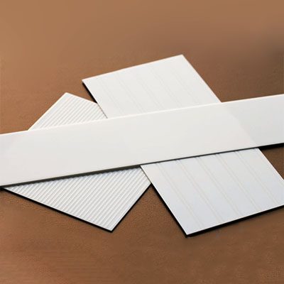
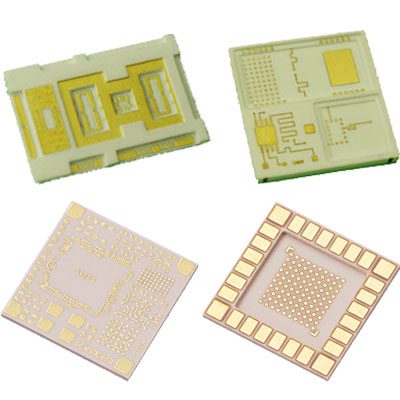
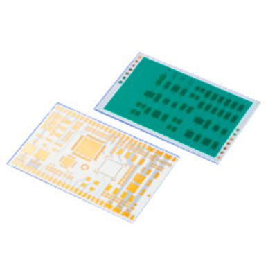
KKPCB is a professional high-precision PCB manufacturing factory based in China, specializing in custom-designed ceramic packages and components to meet specific customer requirements. Our standard product offerings include DBC substrates, AMB substrates, thick-film ceramic substrates, LTCC substrates, high-power module substrates, general module substrates, RF/microwave ceramic substrates, sensor and medical device substrates, and automotive electronics substrates.
Performance required for ceramic substrates and packages
Ceramic substrates and IC packages are used for semiconductor packages and electronic modules, of which the speedy operation and high integration are advancing, and sensor modules, of which the high precision and high sensitivity is advancing.
The performance required for these applications is as follows.
- Dimensional stability and flatness
- Supports various mounting forms (wire bonding, flip chip bonding, SMT, etc.)
- The coefficient of linear expansion is close to that of silicon
- Small size with fine wiring
- Frequency characteristic
- High reliability including heat resistance and humidity resistance
Listed below are KOA’s LTCC boards that satisfy the above conditions.
Applications of LTCC substrates
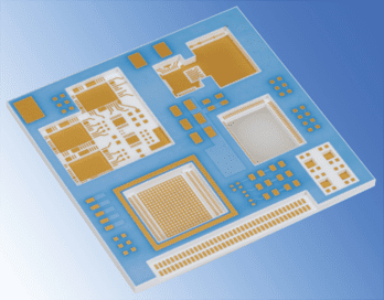
- Microwave and millimeter-wave substrate for high frequency module
- Interposer for semiconductor packages
- Sensor module package such as MEMS
- High reliability module for aerospace and industrial applications
Click here for the product information on LTCC substrate
Features of KLC series (LTCC substrate)
- Low dielectric loss characteristics (tan δ) and low resistance conductor with small electrical loss, which is suitable for high frequency applications
- Less variation in size and characteristics of each production lot and within each lot due to our unique manufacturing technology
- High-density wiring realized by improved stacking alignment accuracy
- Accurate control of substrate thickness and cavity shape
- Built-in resistor, inductor, and capacitor functions in the substrate and package
High frequency applications
LTCC substrates is a type of ceramic multilayer substrate. It is fired at a lower temperature than a high-temperature fired ceramic substrate (HTCC substrate) whose main component is alumina, and Ag. And it uses Ag, which has the low conductor resistance, as a inner layer conductor. Followings are the electrical characteristics it has.
- Low dielectric loss (tan δ)
- Low conductor resistance )
Low dielectric loss and low conductor resistance lead to low electrical loss at the high frequencies. Having lower dielectric loss than resin substrates, and the conductor with better electrical conduction than that of HTCC substrates, it is generally the most suitable choice for the high-frequency applications.
KKPCB develops and provides a wide variety of ceramics for package applications. Material properties of typical multilayer ceramics are as follows:
| CERAMIC MATERIAL OPTIONS | ELECTRICAL | THERMAL | MECHANICAL | CONDUCTOR MATERIAL | ||||||
|---|---|---|---|---|---|---|---|---|---|---|
| Dielectric Constant | Dielectric Loss Angle (x1.0E-4) | CTE(ppm/K) (RT-400°C) | Thermal Conductivity (W/mK) | Flexural Strength (MPa) | Young’s Modulus of Elasticity (GPa) | |||||
| 1MHz | 2GHz | 1MHz | 2GHz | |||||||
| Alumina (Al2O3) | A473 | 9.1 | 8.5 | 5 | 10 | 6.9 | 18 | 400 | 270 | W, Mo |
| A440 | 9.8 | _ | 24 | _ | 7.1 | 14 | 400 | 310 | W, Mo | |
| A443 | 9.6 | _ | 5 | _ | 6.9 | 18 | 460 | 310 | W, Mo | |
| AO610W | 9.2 | 9.0 | 9 | 11 | 6.9 | 17 | 460 | 281 | CuW | |
| AO630 | 9.3 | 9.1 | 5 | 23 | 7.0 | 16 | 460 | 275 | CuW | |
| AO700 | 9.4 | 9.2 | 6 | 6 | 7.2 | 21 | 620 | 315 | Mo | |
| AO800 | 9.4 | 9.4 | 4 | 13 | 7.5 | 16 | 740 | 300 | CuW, Mo | |
| AlN | AN242 | 8.7 | 8.6 | 1 | 170 | 4.7 | 150 | 400 | 320 | W |
| LTCC | GL570 | 5.6 | 5.7 | 3 | 7 | 3.4 | 2.8 | 200 | 128 | Cu |
| GL580 | 6.2 | 6.1 | 4 | 16 | 10.4 | 2.0 | 270 | 103 | Cu | |
| GL771 | 5.3 | 5.2 | 8 | 36 | 12.3 | 2.0 | 170 | 74 | Cu | |
| GL773 | 5.7 | 5.8 | 5 | 23 | 11.7 | 1.9 | 280 | 95 | Cu | |
- Material characteristics mentioned above are typical values.
These values may change upon further improvement or modification of these materials and processes.
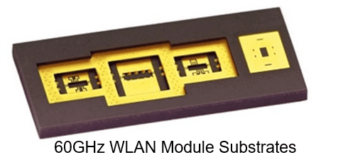
Millimeter-wave module
At high frequencies such as millimeter wave, the LTCC substrate has the advantage over the fluororesin substrate in the easiness of multilayering.
It also provides the following benefits:
- Since the coefficient of thermal expansion is close to that of silicon, the Si-based semiconductor bare chip can be mounted easily.
- High heat dissipation due to higher thermal conductivity by one digit compared with fluororesin substrate
- High moisture resistance due to its non-water-absorbing characteristic
- High-precision cavity formation enables downsizing
Above characteristics show that the LTCC substrates are suitable for semiconductor mounting, modules and packages for millimeter-wave band.
Cavity formation for packages
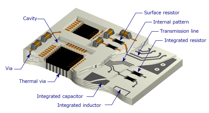
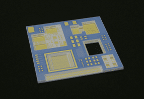 Cavity refers to the hollow space formed on a substrate, where semiconductor, sensor and other components are mounted. It enables the downsizing of module and the improvement of its characteristics.
The high dimensional accuracy of cavity and the forming of complex cavity shapes are available on KOA’s LTCC. Also, the positioning accuracy of the pads for component mounting is high, making it suitable for flip-chip mounting.
It also supports complex cavity shapes for multi-chip packages.
Improvement of the heat dissipation by thermal via
For semiconductor chips that generate a large amount of heat, thermal conductivity and heat dissipation can be improved by forming a thermal via directly under them.

Structure of LTCC substrate
The figure below is an example of a module using the LTCC substrate.
Inner layer wiring is formed on each layer and the layers are connected by via holes. Inductors, capacitors and strip lines for high frequencies can be formed in the LTCC substrate with a ceramic multilayer structure.
Manufacturing process
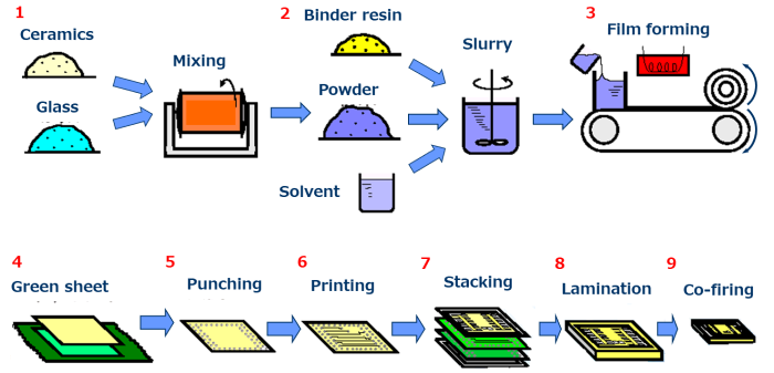
- Ceramics and glass powder are mixed.
- An organic binder and solvent are added to the mixed raw materials and dispersed until they become uniform. It makes a material called slurry, which is the basis of a green sheet.
- Slurry is spead on the PET film and dried in the oven to roll-up. This sheet raw ceramics is called “green sheet”
- Green sheet is cut-out to the square shape.
- Through holes are created to make via holes for electrical conductivity.
- Via holes are filled and circuit pattern is printed on the green sheet.
- Several layers are prepared and stacked to make multilayer circuit.
- Sheet block is laminated and fired to make LTCC multilayer substrate.
- Surface of the substrate is plated, and then substrate is separated into pieces depending on requirements.
Manufacturing Process:
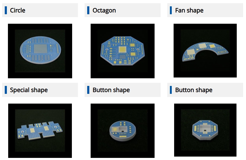
Custom shape package (example)
Ceramic Substrates Frequent Questions
A ceramic substrate is a type of material used in electronic components that provides support and electrical insulation. It is typically made from ceramic materials such as alumina (Al₂O₃), aluminum nitride (AlN), or silicon nitride (Si₃N₄). Ceramic substrates are widely used in applications that require high thermal conductivity, high temperature resistance, and electrical insulation.
Key Features of Ceramic Substrates:
- Thermal Conductivity: Ceramic substrates can efficiently dissipate heat, making them ideal for high-power and high-heat applications.
- High Temperature Resistance: They can operate in high-temperature environments without degrading, which is crucial for power electronics and industrial applications.
- Electrical Insulation: Ceramic materials offer excellent electrical insulation properties, which helps in preventing short circuits and electrical failures.
- Mechanical Strength: Ceramics are hard and have high strength, providing durability and reliability in harsh conditions.
Common Applications:
- Power Modules: For high-power electronics like LEDs, power amplifiers, and laser diodes.
- Automotive Electronics: In sensors, power management systems, and other high-temperature automotive applications.
- Communication Devices: Used in RF/microwave components and antenna systems.
- Medical Devices: For sensors and other critical components in medical equipment.
Overall, ceramic substrates are essential in the manufacturing of high-performance, reliable, and durable electronic components across various industries.
Ceramic substrates are made from a variety of materials, each chosen for its specific properties such as thermal conductivity, electrical insulation, and mechanical strength. The most common materials used for ceramic substrates include:
-
Alumina (Al₂O₃):
- Properties: Excellent electrical insulation, good thermal conductivity, high mechanical strength, and resistance to high temperatures.
- Applications: Widely used in power electronics, sensors, LED modules, and telecommunications.
-
Aluminum Nitride (AlN):
- Properties: Superior thermal conductivity (higher than alumina), good electrical insulation, and high-temperature resistance. Aluminum nitride is ideal for applications requiring effective heat dissipation.
- Applications: Used in high-power electronic devices, laser modules, and microelectronic packaging.
-
Silicon Nitride (Si₃N₄):
- Properties: High thermal conductivity, excellent mechanical strength, and resistance to thermal shock. Silicon nitride is often used in extreme environments.
- Applications: Typically used in high-performance electronics, automotive applications, and high-frequency circuits.
-
Beryllium Oxide (BeO):
- Properties: Exceptional thermal conductivity and electrical insulation, but more hazardous to handle due to the toxicity of beryllium dust.
- Applications: Used in high-power electronics, aerospace, and military applications where thermal management is critical.
-
Zirconia (ZrO₂):
- Properties: Good thermal insulation, high strength, and resistance to wear. Zirconia is often chosen for its durability and high-performance capabilities.
- Applications: Used in specialized applications like gas sensors and high-performance industrial devices.
-
Magnesium Oxide (MgO):
- Properties: Good thermal conductivity and electrical insulation, though less common than other ceramic materials.
- Applications: Sometimes used in lower-power electronics and less demanding applications.
These materials are chosen based on the specific requirements of the application, such as the need for high thermal conductivity, resistance to high temperatures, or electrical insulation. Ceramic substrates are essential in high-power, high-frequency, and high-temperature electronics where standard PCB materials would not perform as well.
Ceramic substrates and regular PCBs (Printed Circuit Boards) differ primarily in materials, performance, and applications.
-
Material Composition:
- Ceramic Substrates: Made from ceramic materials like alumina (Al₂O₃), aluminum nitride (AlN), or silicon nitride (Si₃N₄). These materials offer excellent thermal conductivity, high temperature resistance, and electrical insulation.
- Regular PCBs: Typically made from materials such as fiberglass-reinforced epoxy (FR4), copper foil, and resin. PCBs are generally used for low-to-medium power applications.
-
Thermal Conductivity:
- Ceramic Substrates: They have superior thermal conductivity, making them ideal for high-power applications where heat dissipation is crucial.
- Regular PCBs: They have lower thermal conductivity and are not suitable for applications with high heat generation unless additional cooling methods are employed.
-
Temperature Resistance:
- Ceramic Substrates: Can withstand higher temperatures (up to 300°C or more), which is essential for high-temperature environments such as power modules, automotive electronics, and industrial applications.
- Regular PCBs: Typically operate at lower temperatures (usually up to 100-150°C), and prolonged exposure to higher temperatures may cause the material to degrade.
-
Electrical Insulation:
- Ceramic Substrates: Offer excellent electrical insulation properties, which makes them suitable for high-voltage applications and sensitive circuits.
- Regular PCBs: Provide good electrical insulation but are not as efficient as ceramic substrates in high-voltage and high-frequency environments.
-
Mechanical Strength:
- Ceramic Substrates: Have high mechanical strength but are more brittle and can break or crack under excessive stress.
- Regular PCBs: Generally softer and more flexible than ceramic substrates, making them more resistant to mechanical shock but less durable in high-stress environments.
-
Applications:
- Ceramic Substrates: Used in high-power, high-temperature, and high-frequency applications such as LED modules, automotive electronics, power devices, industrial sensors, and medical devices.
- Regular PCBs: Commonly found in consumer electronics like smartphones, computers, home appliances, and other general electronics with lower power and temperature requirements.
-
Cost:
- Ceramic Substrates: Due to the specialized materials and manufacturing processes, ceramic substrates are more expensive.
- Regular PCBs: Cost-effective and mass-produced, making them suitable for consumer electronics and large-scale applications.
In summary, ceramic substrates are ideal for demanding applications that require superior heat management, electrical insulation, and high-temperature performance, while regular PCBs are more suitable for everyday consumer electronics and less demanding environments.
The surface treatment of ceramic substrates is crucial for improving their adhesion, conductivity, and reliability, as well as enhancing the performance of the final product. Common surface treatment processes for ceramic substrates include:
-
Plating:
- Process: A thin metal layer, typically copper or gold, is plated onto the ceramic substrate's surface to enhance its electrical conductivity and ensure strong interconnection with other components.
- Applications: Used in high-frequency and high-power applications, such as power modules and RF circuits.
-
Solder Masking:
- Process: A solder mask is applied to the ceramic surface to protect specific areas from soldering and to prevent oxidation. The mask helps define the areas where soldering should occur.
- Applications: Commonly used in electronic devices where precision soldering is required, such as in module assemblies.
-
Lapping and Polishing:
- Process: The surface of the ceramic substrate is ground or polished to a smooth finish using abrasives. This enhances surface flatness, reduces surface roughness, and improves adhesion during the bonding process.
- Applications: Used for high-precision applications where a smooth, uniform surface is critical for bonding or component mounting.
-
Coating (Dielectric Coating):
- Process: A dielectric coating, such as a layer of resin or ceramic material, is applied to improve insulation and protect the ceramic surface from environmental factors like moisture and contamination.
- Applications: Applied to substrates used in high-voltage or sensitive applications, ensuring the substrate maintains electrical insulation and durability.
-
Etching:
- Process: Chemical etching is used to pattern or clean the ceramic substrate's surface. It can be used to create microstructures or remove unwanted material to improve surface properties or prepare for further processing.
- Applications: Often used in the fabrication of microelectronic components or to create fine features on ceramic substrates.
-
Laser Ablation:
- Process: A laser is used to selectively remove material from the ceramic substrate to create specific patterns or to expose metal layers for further processing. This process offers high precision and can be used for very fine features.
- Applications: Used in precision electronics and components requiring detailed patterning or micro-structuring.
-
Bonding (e.g., Active Metal Brazing, Diffusion Bonding):
- Process: Metal is bonded to the ceramic surface using methods such as active metal brazing or diffusion bonding to improve the substrate’s mechanical strength and electrical connection with other components.
- Applications: Used in power modules and electronic assemblies where a strong, reliable connection is essential.
These surface treatment processes ensure that ceramic substrates meet the performance and reliability requirements of various applications, such as power electronics, automotive systems, telecommunications, and medical devices. The choice of treatment depends on the specific needs of the application, including factors like electrical conductivity, thermal management, and mechanical durability.
Testing ceramic substrates is essential to ensure they meet the required performance standards for electrical, thermal, and mechanical properties. The main testing methods for ceramic substrates include:
-
Visual Inspection:
- Process: A thorough visual examination is done to check for surface defects such as cracks, chips, or discoloration. This step ensures that the substrate is physically intact before further testing.
- Applications: Initial quality control to detect visible defects in mass production.
-
Dimensional Measurement:
- Process: Precision tools like calipers, micrometers, or coordinate measuring machines (CMM) are used to verify the substrate's dimensions (length, width, thickness).
- Applications: Ensures that the ceramic substrate meets the specified size and tolerance requirements for proper fitting in electronic assemblies.
-
Thermal Conductivity Testing:
- Process: The thermal conductivity of the ceramic substrate is tested using techniques like the hot disk method or laser flash analysis. This is crucial for substrates used in high-power or high-heat applications.
- Applications: Essential for power electronics, LED modules, and high-frequency devices where heat dissipation is a critical factor.
-
Electrical Insulation Testing:
- Process: Electrical tests, such as dielectric strength tests or insulation resistance tests, are performed to measure the substrate's ability to insulate against electrical current.
- Applications: Used to ensure the substrate provides adequate electrical insulation for high-voltage or sensitive electronics applications.
-
High-Temperature Testing:
- Process: The ceramic substrate is exposed to high temperatures to assess its performance under extreme conditions. This includes checking for thermal expansion, dimensional stability, and resistance to heat-induced damage.
- Applications: Important for automotive, industrial, and aerospace applications where substrates must endure high-temperature environments.
-
Mechanical Strength Testing:
- Process: Mechanical tests, such as bending strength, compression, or fracture toughness tests, are conducted to measure the substrate's mechanical durability and resistance to breakage.
- Applications: Ensures that the ceramic substrate can withstand mechanical stress during handling and operation, especially in high-stress applications.
-
Surface Roughness Measurement:
- Process: Surface roughness is measured using profilometers or other precision equipment to ensure that the substrate has the appropriate surface finish for bonding or component mounting.
- Applications: Ensures optimal surface preparation for soldering, bonding, or component adhesion.
-
Bonding Strength Testing:
- Process: The strength of the bond between the ceramic substrate and its metal or component layers is tested through shear, peel, or tensile strength tests.
- Applications: Important for ensuring the reliability of electrical and mechanical connections, especially in power modules and high-performance electronics.
-
X-Ray Inspection:
- Process: X-ray imaging is used to detect internal defects, such as voids, cracks, or poor metal bonding that might not be visible on the surface.
- Applications: Used for high-precision applications where internal structural integrity is critical, such as in medical devices and high-reliability electronics.
-
Environmental Testing:
- Process: Environmental tests, such as humidity exposure, thermal cycling, or salt spray testing, are performed to assess how the ceramic substrate performs under different environmental conditions.
- Applications: Important for automotive, aerospace, and military applications where substrates may be exposed to harsh environmental factors.
These tests ensure that ceramic substrates perform reliably in their intended applications, especially in high-performance electronics, automotive systems, power modules, and medical devices. By evaluating a variety of mechanical, electrical, and thermal properties, manufacturers can confirm that the ceramic substrates meet the required quality and performance standards.
Ceramic substrates are widely used across various industries due to their excellent thermal conductivity, electrical insulation, high-temperature resistance, and mechanical strength. The primary industries that use ceramic substrates include:
-
Power Electronics:
- Applications: Power modules, inverters, converters, and motor control circuits.
- Why: Ceramic substrates are used in power electronics to manage high power levels and dissipate heat efficiently, ensuring the stability and performance of power devices.
-
Automotive Electronics:
- Applications: Engine control units (ECUs), power management systems, sensors, lighting, and safety systems.
- Why: Automotive applications require reliable components that can withstand extreme temperatures and harsh conditions, making ceramic substrates ideal for these applications due to their thermal and mechanical properties.
-
Telecommunications:
- Applications: RF (radio frequency) components, antennas, power amplifiers, and communication modules.
- Why: Ceramic substrates offer high thermal conductivity and electrical insulation, which are critical in RF and microwave applications for reliable performance and heat management.
-
LED Lighting:
- Applications: High-power LED modules and lighting systems.
- Why: Ceramic substrates, particularly those made of aluminum nitride (AlN) or alumina (Al₂O₃), are commonly used in LED modules due to their excellent heat dissipation capabilities, which are essential for preventing overheating and improving the lifespan of LEDs.
-
Medical Devices:
- Applications: Sensors, diagnostic equipment, implantable devices, and medical imaging systems.
- Why: Ceramic substrates are used in medical devices for their biocompatibility, high reliability, and performance in harsh conditions, ensuring the safety and longevity of critical medical equipment.
-
Aerospace and Defense:
- Applications: Radar systems, satellite components, sensors, and avionics.
- Why: In aerospace and defense, ceramic substrates are valued for their ability to withstand extreme temperatures and mechanical stress while providing reliable electrical insulation and heat management in demanding environments.
-
Consumer Electronics:
- Applications: High-performance microelectronics, circuit boards for smartphones, laptops, and other electronic devices.
- Why: Ceramic substrates are used in consumer electronics to enhance the performance and reliability of high-frequency and high-power components, ensuring device longevity and efficiency.
-
Industrial Equipment:
- Applications: Industrial control systems, power supplies, motor drives, and process monitoring equipment.
- Why: The durability and reliability of ceramic substrates make them suitable for industrial applications that require high performance in challenging environments.
-
Renewable Energy:
- Applications: Solar inverters, energy storage systems, and wind turbine electronics.
- Why: Ceramic substrates are used in renewable energy applications for their ability to handle high-power demands, dissipate heat, and operate under varying environmental conditions.
-
Sensors and IoT Devices:
- Applications: Gas sensors, temperature sensors, pressure sensors, and smart devices.
- Why: The high sensitivity and reliability of ceramic substrates make them ideal for sensors in Internet of Things (IoT) devices, where precise measurements and long-term durability are required.
-
High-Frequency and Microwave Electronics:
- Applications: Microwave circuits, RF power amplifiers, and oscillators.
- Why: Ceramic substrates with high thermal conductivity and low dielectric loss are essential for maintaining performance in high-frequency and microwave applications, preventing heat buildup and ensuring stable operation.
Ceramic substrates play a critical role in industries that demand high performance, reliability, and durability. Their ability to handle high temperatures, high power, and provide electrical insulation makes them an essential component in a wide range of advanced applications across various sectors.
Designing ceramic substrates involves several challenges due to the unique properties of ceramic materials and the specific requirements of the applications. Key challenges include:
-
Material Selection:
- Challenge: Choosing the right ceramic material for the substrate is critical. Different ceramics (e.g., alumina, aluminum nitride, silicon nitride) have varying thermal conductivity, dielectric properties, and mechanical strength. The material must meet the specific requirements of the application, such as high thermal conductivity for power electronics or electrical insulation for high-voltage components.
- Solution: Careful selection based on the application’s thermal, electrical, and mechanical needs is necessary. This requires in-depth knowledge of material properties and the specific demands of the end product.
-
Thermal Management:
- Challenge: Effective heat dissipation is a primary concern, especially for high-power applications. Ceramic substrates are used for their thermal conductivity, but ensuring proper heat flow from sensitive components to the substrate without causing thermal stress is difficult.
- Solution: Incorporating proper design features such as heat sinks, vias, and careful placement of heat-generating components can help optimize heat distribution and avoid thermal damage.
-
Mechanical Strength and Fragility:
- Challenge: Ceramics are generally brittle and can fracture or crack under stress or improper handling. Ensuring that the substrate can withstand mechanical stresses during manufacturing, assembly, and operation without failure is challenging.
- Solution: Designing with appropriate thickness, using reinforcement methods, and ensuring proper handling and transport procedures can help mitigate mechanical fragility.
-
Surface Preparation and Bonding:
- Challenge: Achieving proper bonding between the ceramic substrate and other materials, such as metals or components, is essential for electrical connections and mechanical integrity. Surface roughness, cleanliness, and the need for special coatings (e.g., solder mask or metallization) can add complexity.
- Solution: Using advanced surface treatment techniques like laser ablation, plating, or sputtering to prepare the ceramic surface ensures strong bonding. Metallization and active metal brazing techniques are often used to create robust metal-to-ceramic bonds.
-
Design for Manufacturability (DFM):
- Challenge: Ceramic substrates often require more complex manufacturing processes than traditional PCBs. The need for precision in cutting, shaping, and surface treatment can make mass production more challenging and expensive.
- Solution: Collaborating closely with manufacturers to understand their capabilities, and designing with manufacturability in mind, can streamline the process and minimize defects or delays in production.
-
Cost Considerations:
- Challenge: Ceramic substrates can be more expensive than traditional PCB materials due to the cost of raw materials, specialized manufacturing processes, and the complexity of surface treatments. Balancing cost with the performance requirements of the application can be difficult.
- Solution: A cost-benefit analysis should be conducted to determine the most appropriate ceramic material and design approach. In some cases, optimizing the design to reduce material waste or simplifying the manufacturing process can help control costs.
-
Precision and Tolerance:
- Challenge: Ceramic substrates often require very tight tolerances to ensure proper fit and function in their applications. Achieving high precision in shaping, cutting, and creating vias or holes can be technically difficult and requires advanced manufacturing capabilities.
- Solution: Using advanced machining techniques like laser cutting, precision grinding, or diamond tools, and implementing strict quality control measures throughout the design and manufacturing processes can help achieve the necessary precision.
-
Environmental Resistance:
- Challenge: Ceramic substrates are often used in harsh environments, such as automotive, aerospace, and industrial applications. Ensuring long-term performance in the face of environmental factors like temperature fluctuations, humidity, vibration, and chemical exposure is crucial.
- Solution: Materials must be carefully selected for environmental resistance, and additional protective coatings or treatments (e.g., conformal coating) may be required to enhance durability in harsh conditions.
-
Miniaturization and High-Density Designs:
- Challenge: As electronics continue to trend towards smaller and more compact designs, integrating high-density circuits on ceramic substrates becomes increasingly difficult. Managing space while maintaining the required electrical performance and thermal management is a significant challenge.
- Solution: Utilizing advanced techniques such as microvias, multi-layer designs, or embedding components within the substrate can help achieve high-density layouts while maintaining functionality and heat dissipation.
-
Testing and Quality Control:
- Challenge: Ensuring the reliability and performance of ceramic substrates involves rigorous testing, including mechanical, electrical, and thermal evaluations. Achieving uniform quality control, especially for critical applications like medical or aerospace electronics, can be challenging.
- Solution: Implementing a comprehensive testing protocol during both the design and production stages, such as X-ray inspection, thermal cycling, and electrical testing, can ensure that substrates meet performance standards.
Designing ceramic substrates requires a deep understanding of materials, advanced manufacturing techniques, and the specific needs of the end application. Overcoming these challenges ensures that the final product performs reliably in demanding environments and meets industry-specific requirements.
Choosing a professional PCB factory to produce ceramic substrates requires careful evaluation of various factors to ensure quality, performance, and reliability. Here are the key considerations when selecting a factory for ceramic substrate production:
-
Experience and Specialization in Ceramic Substrates:
- Why It Matters: Ceramic substrates require specialized manufacturing techniques, and not all PCB factories have the expertise to produce them. A factory with experience in ceramic materials will have the necessary knowledge and skills to produce high-quality substrates.
- What to Look For: Look for a factory that specializes in ceramic substrates and has a proven track record in manufacturing high-performance ceramics for industries such as power electronics, automotive, telecommunications, and medical devices.
-
Material Selection and Knowledge:
- Why It Matters: Different ceramic materials (e.g., alumina, aluminum nitride, silicon nitride) have distinct properties that suit various applications. A professional PCB factory should have extensive knowledge of the different types of ceramics and their performance characteristics.
- What to Look For: Ensure the factory offers a range of ceramic materials and provides guidance on selecting the most suitable material based on your application requirements for thermal conductivity, dielectric properties, and mechanical strength.
-
Advanced Manufacturing Capabilities:
- Why It Matters: Ceramic substrates often require advanced manufacturing processes like laser cutting, metallization, high-temperature firing, and precise machining. The capabilities of the factory directly impact the quality and performance of the final product.
- What to Look For: Verify that the factory has state-of-the-art equipment, such as laser ablation machines, high-precision cutting tools, and automated metallization systems, to ensure high precision and quality control in the production process.

