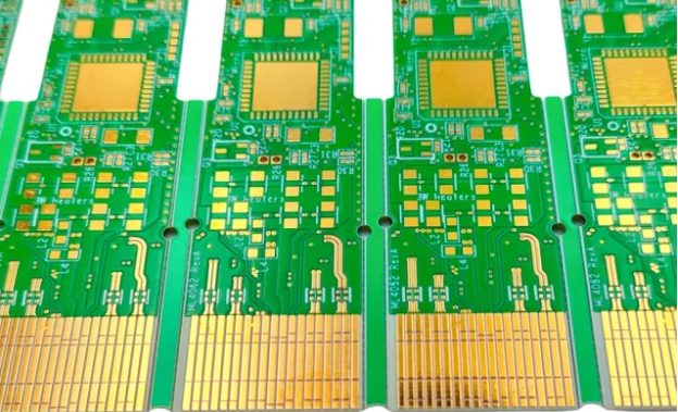
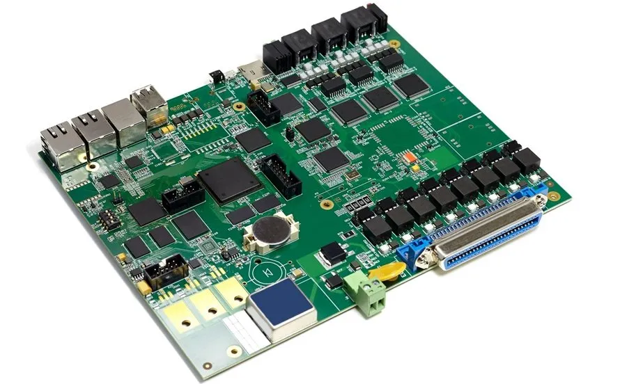
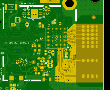
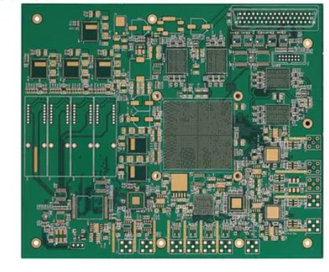
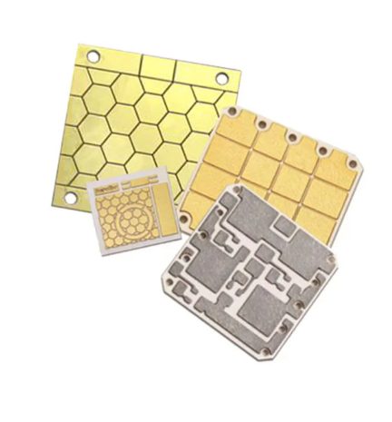
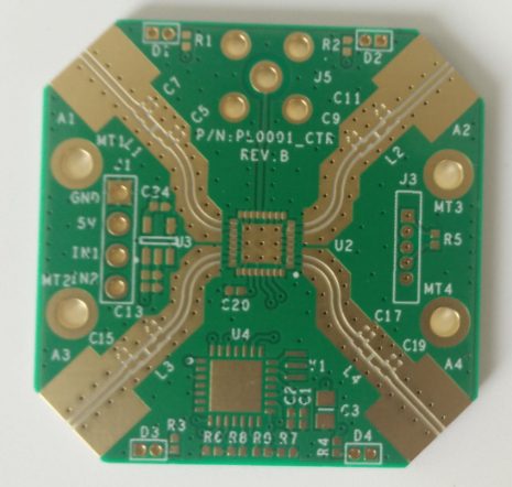
High frequency PCBs are specialized circuit boards designed to transmit signals over a gigahertz (GHz) frequency range, ensuring quick and reliable communication in devices ranging from military radar systems to smartphones.
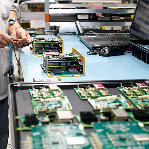
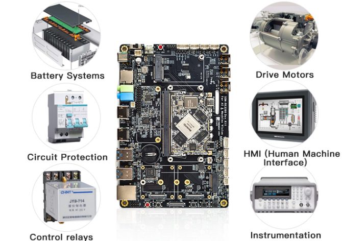
The Printed Circuit Board (PCB) is a fundamental component of all electronic devices, serving as the “command center” that ensures their functionality. However, many business owners struggle to differentiate between PCB manufacturing and PCB assembly, often leading to suboptimal decisions.
In the world of PCB manufacturing, two main methods are commonly used: PCB prototyping and standard PCB production. Both methods play critical roles and come with their own characteristics. Reducing the time and costs associated with the development process can significantly increase the success rate of future projects. This article explores the benefits of starting with a prototype PCB for design verification before transitioning to standard PCB production assembly.
The client specializes in the development and production of a wide range of microwave electronic products. These products are extensively used in satellite communication, television broadcasting, long-range communication, data and image transmission, radar, remote control, remote sensing, electronic reconnaissance, and electronic countermeasures. With deep technical expertise in microwave technology and high-frequency electronic products, the customer serves multiple high-tech industries requiring precise, reliable, and high-frequency transmission solutions.
Whether in the PCB manufacturing assembly process or in actual applications, good materials are essential for the reliable performance of PCBs. Because defects in PCB assembly may cause failures in actual product applications, resulting in immeasurable losses. Therefore, we should not only pay attention to the cost of PCB production, but also the materials and quality of PCBs.
The high coefficient of thermal expansion of ceramic PCB substrates is one of the reasons for their widespread use in the electronics industry. The thermal conductivity of ceramic bases stems from its proximity to silicon while being located below the most commonly used connecting metals.
A high-frequency PCB is very similar to any other form of PCB (printed circuit board). It is compatible with microwave radio frequency communications, ranging from five hundred megahertz to two thousand gigahertz.
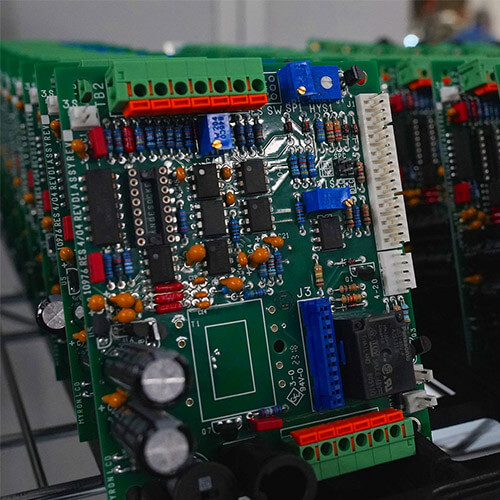
A printed circuit board (PCB) consists of an insulating board on which copper layers and signal lines are etched or printed. The number of layers on an industrial PCB can range from one to eight or more as the complexity of the circuit increases.
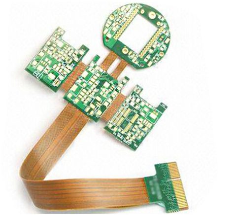
The design of any type of PCB is where everything starts, as assembly may be more efficient there. You must take a close look at all the steps involved in manufacturing a flex-rigid or flexible PCB. Keep in mind that developing a rigid-flex PCB is more complex than a flexible PCB.
Evolution of Medical PCB Assembly
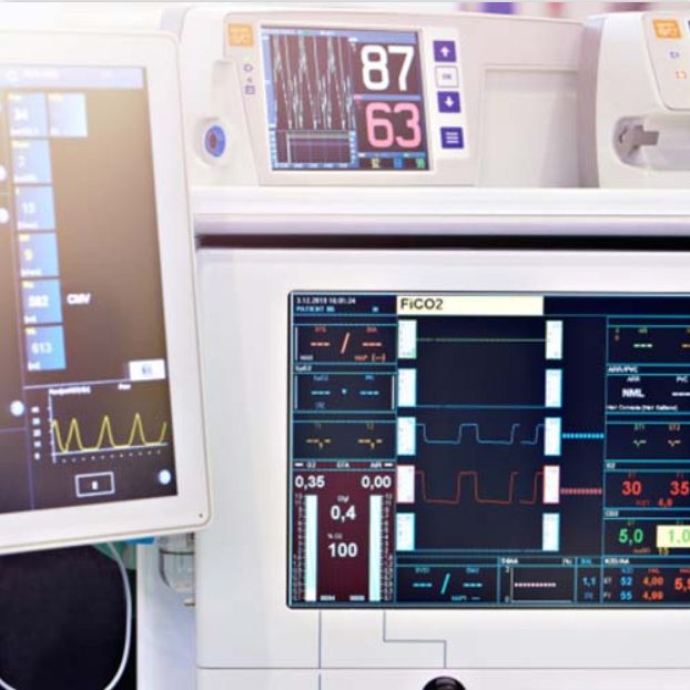
There is more to the advancement of technology and medical devices, and people may no longer need the services of hospitals and doctor’s offices. Medical PCB services are a result of evolution that makes medical operations easier and more stress-free. Diagnosis is one of the key steps to fully utilize these electronic devices to minimize treatment time and increase treatment efficiency.

