N4800-20 is a high-performance enhanced epoxy systems for multilayer PCBs requiring maximum thermal and stable electrical performance. It is designed to be lead-free assembly compatible and CAF resistant.
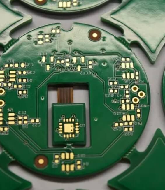
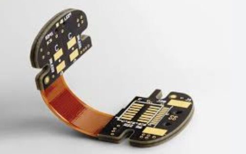
Gangrou combined with print circuit boards allows you to have the advantages of both the beauty. The rigid soft combination of PCB combines the flexibility of the flexible circuit and the durability of the rigid PCB. Flexible printing circuit boards are only flexible materials, which are usually based on polyimide or polyester. They can be single, double or multi -layer boards. The rigid soft combination of PCB also uses flexible and rigid materials. The flexible layer is sandwiched between the rigid layer. The rigid layer has conductors and plating holes to connect the flexible layer to other layers.
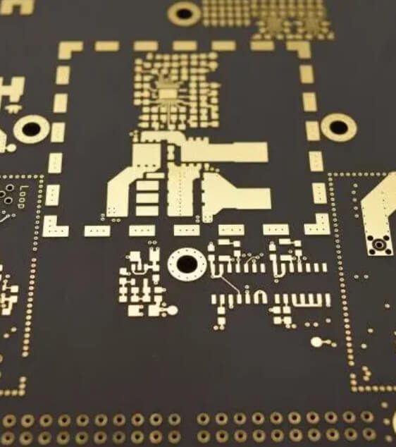
RF and microwave signals are very sensitive to noise -much more sensitive than high -speed digital signals. This means that you need to minimize the noise, bell, and reflection, and at the same time be careful to deal with the entire system.
Returning the signal with the least inductance -the ground floor below the signal will be easier to ensure this path.
Discipline matching is important. With the rise of RF and microwave frequency, the tolerance will become smaller. Generally, the PCB drive needs to be fixed, such as 50 ohms, which means that during the transmission and sending to the receiver, the drive outputs 50 ohms.
The transmission line that is curved due to wiring restrictions should use a curved radius that is at least three times larger than the central conductor width. This will minimize characteristic impedance.
It is necessary to minimize the return loss, whether it is reflected by the signal or the bell. There will always be a return path, but your design should guide it and prevent the return from multi -layer leakage through the PCB.
HDI PCBs have a higher density per unit circuit than traditional PCBs. They use a combination of buried and blind vias and microvias (0.006 inches in diameter or less). A high-density board is a PCB that has one or more of the following features:
These PCBs create a more challenging design for rigid-flex manufacturers, but we’ve been able to supply successful designs with full compliance and reliability. By engineering these in a 3D environment, we’re able to achieve spatial efficiency and incorporate folds and flexes to help you meet the desired shape that works best with your application.
Rigid PCBs are inherently versatile and are suitable for a variety of configurations from single to multi-layer. With KKPCB’s design for manufacturability and engineering services, you can find a rigid PCB that matches your size, material, and build specifications.
Each rigid and flexible printed circuit board (PCB) design is different and can be customized based on the purpose of the board. The same is true for the PCB substrate – fiberglass is a commonly used substrate, but aluminum-based PCBs are also very effective in many industrial applications. Aluminum-based PCBs consist of a metal-based, copper-clad laminate that provides high performance, including excellent electrical insulation and thermal conductivity.
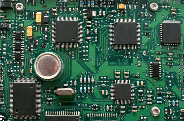
PCB layering or stacking is a way of stacking multiple printed circuit boards together while ensuring that there are predefined interconnections between them, allowing multiple printed circuit boards to be installed in the same device. These multi-layer PCBs can multiply the speed and functionality of a device and are composed of at least three conductive layers, with the bottom layer being composited with an insulating board.
Microstrip patch antennas and their arrays may be rare but are the most widely used antenna form. They have a simple structure and can be formed by a dielectric, a metal conductor patch on the dielectric layer, and a ground plane. Even the dielectric in the middle can be an air structure. A typical microstrip patch antenna is made on a printed circuit board (PCB), and a fine line structure is etched on the conductive metal layer using a photocopying method
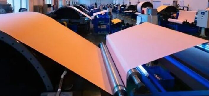
Copper foil used in the PCB industry is more complex than you might think. Copper is both an excellent conductor of electricity and an excellent conductor of heat, making it an ideal conductor for most PCB applications. Copper foil has many other properties that are important for engineers to understand.


