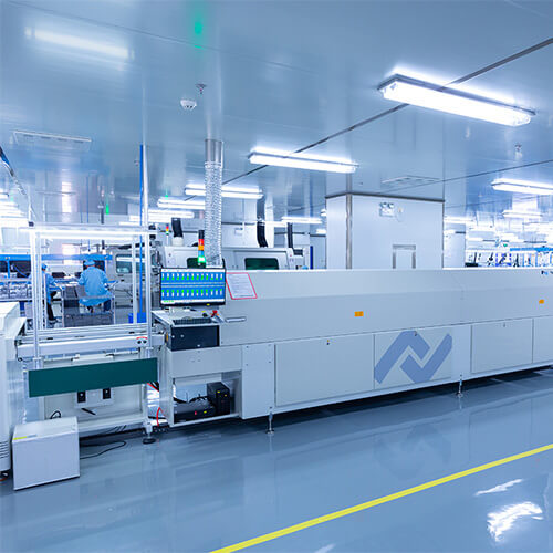
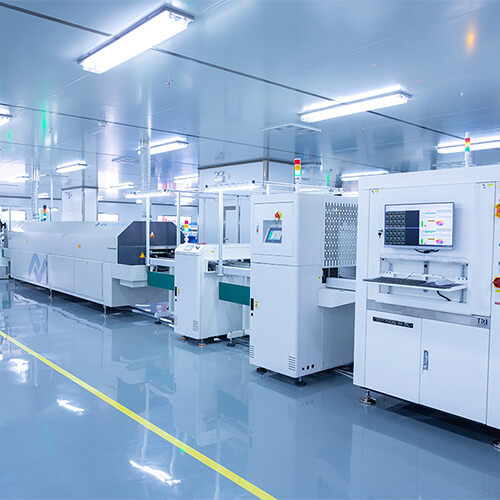
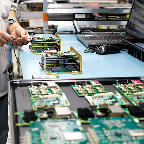
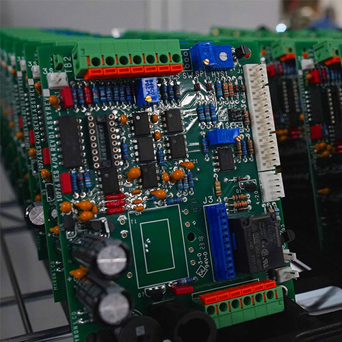
Electronic devices have transformed modern life, and at the heart of these innovations lies a critical component: the Printed Circuit Board (PCB). From smartphones and laptops to industrial machinery and household appliances, PCBs are the backbone of electronics, enabling functionality, precision, and reliability. What Is a PCB? A Printed Circuit Board (PCB) is a thin […]
A multilayer PCB, or Printed Circuit Board, is an advanced type of circuitry that facilitates complex electronic functionalities within a compact framework.
The Curamik® product suite offers best-in-class metallized ceramic substrates for higher power efficiency. Composed of pure copper bonded or brazed to a ceramic substrate, our curamik® substrates are designed to carry higher currents, provide higher voltage isolation, and operate over a wide temperature range.
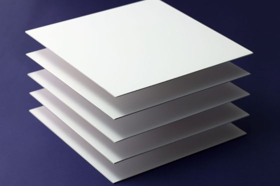
Compared to traditional fiberglass boards, ceramic substrates offer superior mechanical strength, high-temperature resistance, and excellent thermal conductivity. In addition, ceramic substrates also exhibit excellent dimensional and chemical stability.
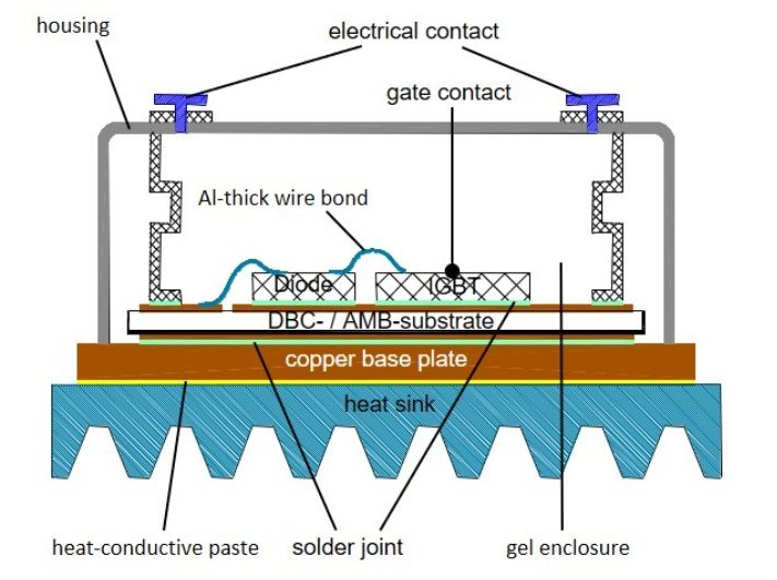
Ceramic substrates are typically located within the copper/metal layers of a power module as part of the power electronics circuitry. They function similarly to a PCB, allowing them to optimally perform their intended purpose
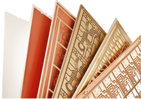
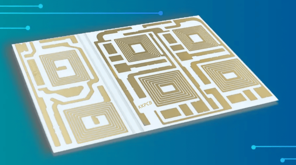
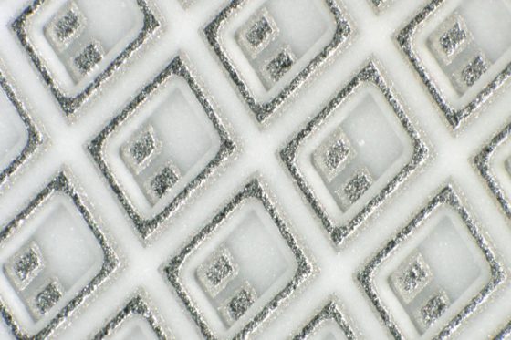
Ceramic PCBs (Ceramic Printed Circuit Boards) are circuit boards that use ceramic materials as substrates, offering excellent thermal management, electrical performance, and mechanical properties. Based on different application requirements and characteristics, ceramic PCBs come in various types, which are outlined below:
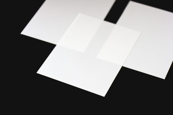
KKPCB’s high-strength flexible Alumina-Zirconia substrates have a bending strength that is more than 1.5 times that of standard alumina substrates. The thinnest thickness can reach 150um, which can reduce thermal resistance in the thickness direction. The substrate has high density, fine structure, and excellent flatness.
A wide range of glaze thicknesses, from 30μm to 200μm. Heat storage and heat dissipation can be controlled by adjusting the glaze thickness. Full-surface glaze or partial-surface glaze designs are available to suit application needs. Wet etching can be used to provide a variety of bump shapes and curvatures. Edge glazed substrates are also available.
The new NIKKO HTCC substrate uses platinum conductor, which is extremely chemically stable and not easy to oxidize, and can be used in various high-temperature environments.
Compatible with SDG, and does not require electroplating for surface treatment, which is low cost.
Bio-friendly material widely used in the medical field.
Provides the catalytic effect of Pt.
Compared with typical HTCC materials, it has higher strength due to the higher alumina content, while having the high thermal conductivity and low dielectric loss of ceramics.
High dimensional tolerance (±0.3%)
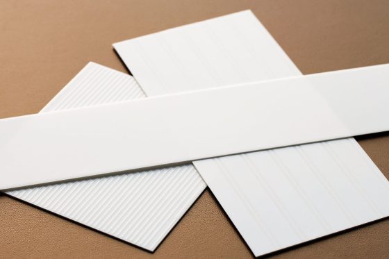
As sintering tool materials – high-purity alumina substrates with excellent surface flatness help improve the characteristics, quality and yield of sintered products. They are also ideal for sintering highly reactive materials. A variety of porosity levels are available due to the ability to control porosity during substrate sintering.

