


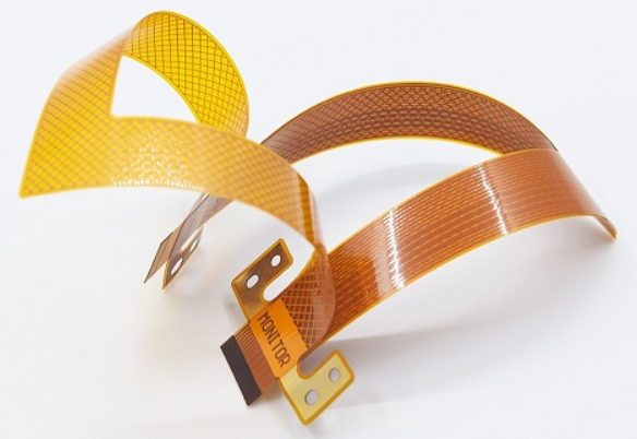
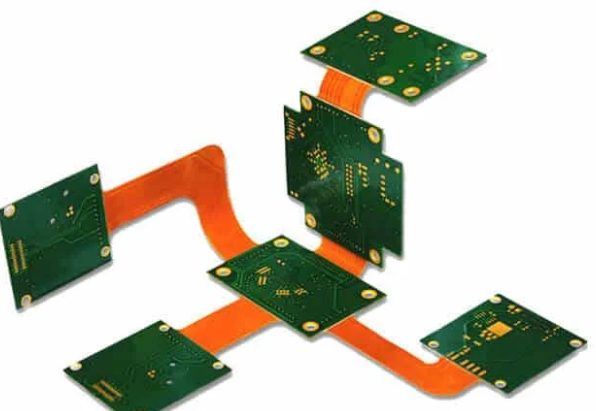
Flexible circuits (also variously referred to around the globe as flex circuits, flexible printed circuit boards, flex print, Flexi-circuits) are members of electronic and interconnection family. They consist of a thin insulating polymer film having conductive circuit patterns affixed thereto and typically supplied with a thin polymer coating to protect the conductor circuits
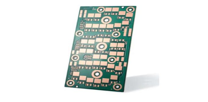
A multilayer PCB is an advanced circuit board featuring multiple layers of conductive copper separated by insulating materials. This configuration is akin to a sandwich, where the copper layers serve as the bread, and the insulating material acts as the filling.
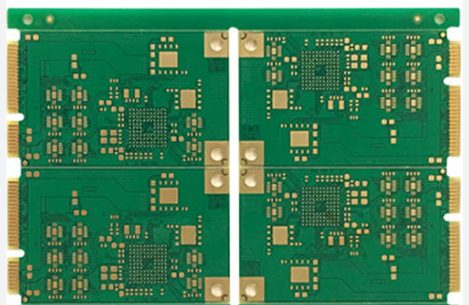
Multilayer PCBs (Printed Circuit Boards) are integral to modern electronics, offering unparalleled performance in compact designs. While they come with several benefits, they also present unique challenges.
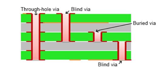
Vias are the copper-plated holes in the PCB that allows the layers to connect. The standard via is called a through-hole via, but there are several disadvantages to using through-hole vias in Surface Mount Technology (SMT). For this reason, we often use a blind via or buried via instead. A blind or buried via can be processed in a wide range of different measures, including plugged copper mask via, a plugged solder mask via, plated via or staggered via
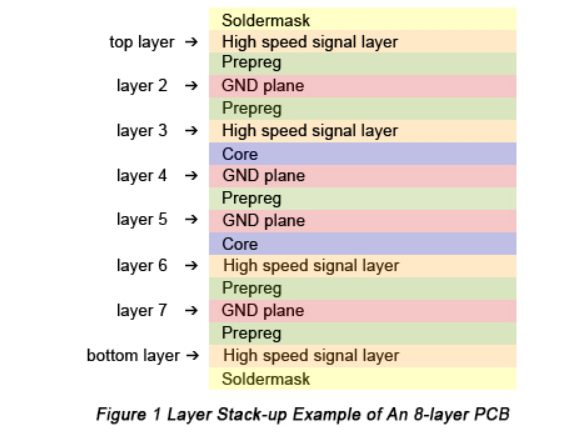
Stack-up refers to the arrangement of copper layers and insulating layers that make up a PCB prior to board layout design. While a layer stack-up allows you to get more circuitry on a single board through the various PCB board layers
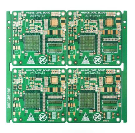
Printed circuit boards (PCBs) are the core of most electronics today, determining basic functions through combinations of components and wiring mechanisms. Most PCBs of the past were relatively simple and limited by manufacturing techniques, while today’s PCBs are much more complex. From advanced flexible options to odd-shaped varieties, PCBs are much more varied in nowadays’ world of electronics
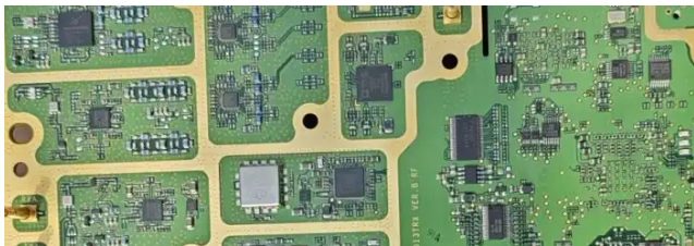
Printed circuit boards (PCBs), or called printed wiring boards (PWBs), have become basic parts in almost all areas of modern technologies. Copper trace is a crucial element on circuit boards. The copper always plays a role of carrying electrical signals to different components across the board assembly. Without traces, the PCB will not function. Of all the elements that build PCB boards, copper is one of the most important.
Printed circuit board (PCB) Prototyping allows engineers to check whether the design will perform as their expectations. At the same time, your PCB prototyping manufacturer would like to check if your circuit boards can be manufactured efficiently. Multiple prototyping runs can be used to test the PCB design variations or to perfect a single function before moving on to the afterwards PCB production stage.
Aluminum PCB, or Aluminium PCB, also called Alu PCB, is one of Insulated Metal Substrate (IMS) PCBs, and is also one of the most commonly used Metal Core PCBs nowadays
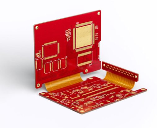
Flexible Printed Circuits (FPCs), also called Flexible Circuits, or Flex Circuits, by IPC definition, a flexible printed circuit is a patterned arrangement of printed circuitry and components that utilizes flexible based material with or without flexible cover lay. This definition is accurate, and conveys some of the potential given the available variations in base materials, conductor materials, and protective cover materials