


The special processes of PCB include but are not limited to the following categories: 1. Ultra-thin board and ultra-thick board: Ultra-thin board refers to a PCB with a thickness smaller than the standard thickness
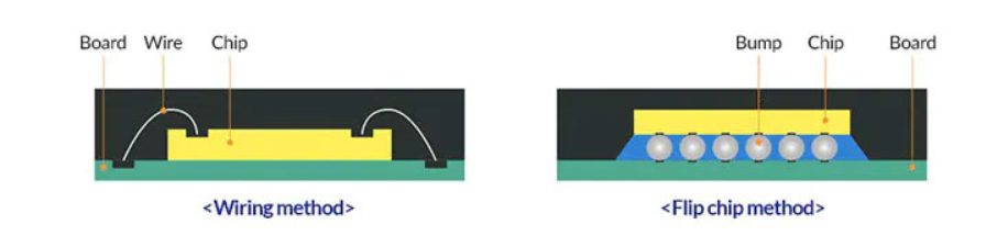
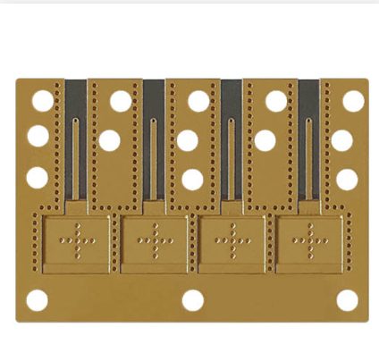
The base material of IC packages is the integrated circuit substrate (or IC package substrate). They shield the bare IC while supporting interconnection between the IC and the PCB’s trace network. As a result, the substrate has a significant impact on circuit performance
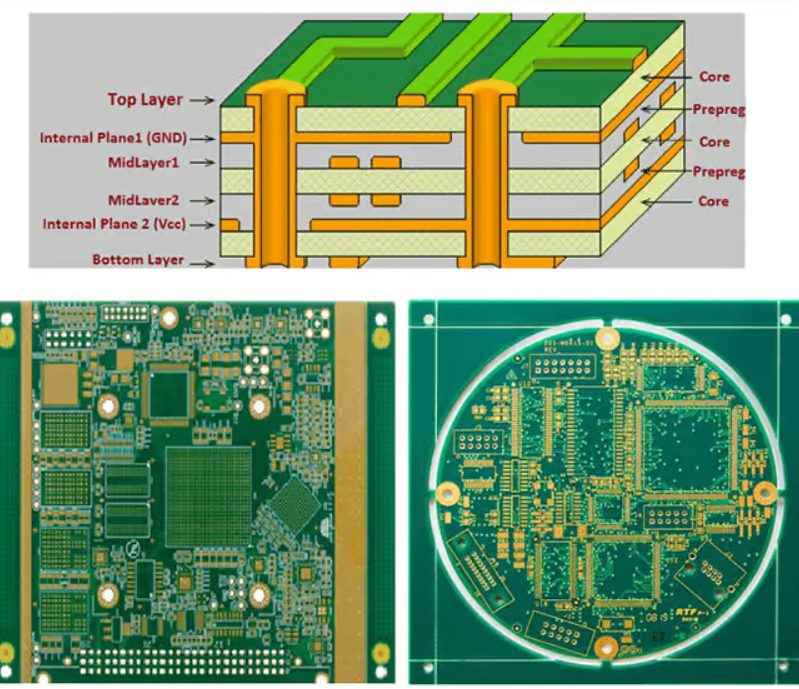
By applying the guidelines in this article around stackup sequence, material selection, hole registration, panelization and thermal management, engineers can fully utilize 10 or more layers for their complex designs. Partnering with a shop experienced in high layer count boards ensures achieving the quality and functionality required to maximize your product’s capabilities and service life.
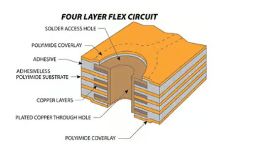
Flexible printed circuits (FPCs) provide invaluable dynamic flexing and shape conforming capabilities in electronics. 4 layer flex PCBs with conductors on 4 layers enable increased routing density and integration versus 2 layer flex, while retaining excellent flexibility.
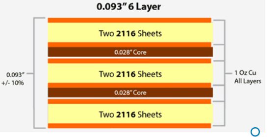
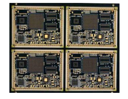
Printed circuit boards (PCBs) have evolved from simple single or double layer boards to complex multilayer boards with 6 or more layers to accommodate increasing component density and interconnectivity needs. 6 layer PCBs provide more flexibility for routing, plane separation and enable partitioning of circuits across layers.
FR4, often written as FR-4, is a widely recognized and high-performing substrate material used in PCB manufacturing. Its affordability, insulation properties, and structural integrity make it the foundation for most PCB designs. FR4 boards are coated with copper foil using adhesive to create conductive layers, either single or double-sided, depending on the design. This flexibility allows for the development of complex multilayer PCBs, making FR4 the default choice for many applications.
Integrated Circuit (IC) substrates are essential components in modern electronics, acting as the primary interface between semiconductor chips and printed circuit boards (PCBs). Their rapid adoption is driven by advanced IC packaging types like Chip Scale Packaging (CSP) and Ball Grid Array (BGA), which demand innovative solutions to meet increasing performance and miniaturization requirements
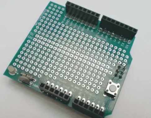
In electronics, prototyping means building an actual circuit to a theoretical design to verify that it works. An electronics designer often builds the first prototype from breadboard or stripboard or perfboard and usually uses them to test circuits. They are generally called prototyping boards.
Flexible Printed Circuit Board (FPCB or Flexible PCB) is a PCB designed to be flexible and can be bent, folded, or twisted. FPC has a combination of multiple printed circuits as well as components located on a flexible substrate. It is usually made of polyimide film material, which ensures high flexibility and thermal stability
Flexible PCB technology, also known as FPC (Flexible Printed Circuit), continues to develop and is used in major electronics sectors such as consumer electronics, automotive, electronic medical devices, wearables, telecommunications and aerospace. The introduction of flexible PCBs has revolutionized conventional electrical interconnect technology, which was traditionally used to connect multiple parts of the same circuit or multiple electronic devices