


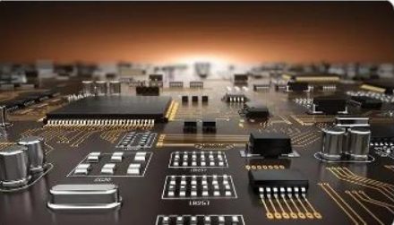
Printed Circuit Boards (PCBs) are the backbone of electronic devices, connecting components seamlessly for reliable functionality. Among these, Flexible LED PCBs have gained prominence due to their adaptability, reduced size, and cost-effectiveness compared to rigid PCBs. They are widely used across industries like consumer electronics, automotive, and aerospace
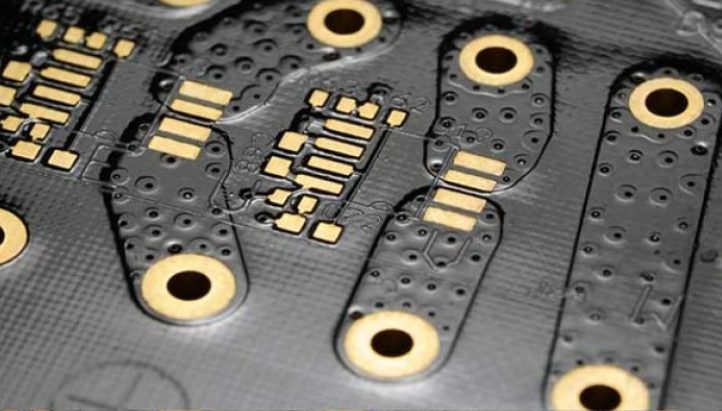
An annular ring refers to the area of copper that surrounds the drilled hole (via) in a PCB. In multi-layer PCBs, vias are essential for connecting various layers. The annular ring ensures strong electrical conductivity between these layers, as it provides the necessary copper coverage around the hole.
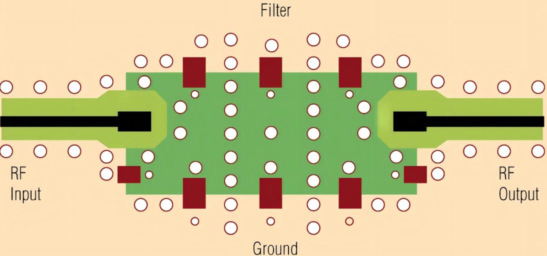
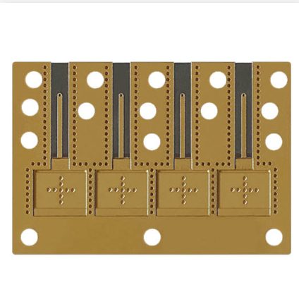
RF PCB refers to a Radio Frequency Printed Circuit Board, operating within a frequency range of 100 MHz to 100 GHz. These specialized PCBs are integral to devices that rely on wireless communication for data transfer.
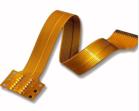
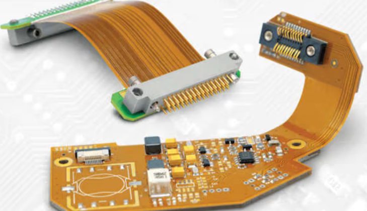
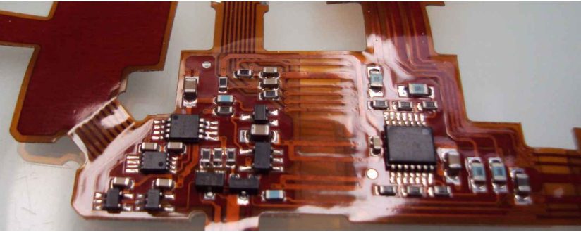
Flexible printed circuit boards (PCBs) are a cornerstone of modern electronics, found in devices like smartphones, cameras, and electric vehicles. Unlike traditional rigid PCBs made from FR4 (flame retardant material), flexible PCBs utilize polymer substrates such as polyimide, resulting in their signature amber or orange appearance
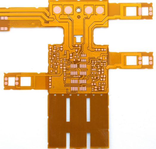
Flexible PCBs (printed circuit boards) provide the ability to bend and conform to various shapes, making them an essential technology for space-constrained and dynamic applications. A 2-layer flex PCB contains a flexible dielectric layer sandwiched between two conductive copper layers. Designing these PCBs requires unique considerations, including material selection, layout techniques, manufacturability, and reliability.
Flexible printed circuit boards (flexible PCBs or flex circuits) are made from flexible insulating materials such as polyimide film. Unlike traditional rigid PCBs, flexible PCBs can bend and twist while maintaining electrical connectivity, making them ideal for space-constrained and dynamic applications.
Special processing technologies are non-conventional processes used in the production of printed circuit boards to meet specific needs. These technologies usually involve high-precision, high-complexity processing requirements and are capable of processing circuit boards with special functions or properties, such as high-frequency PCBs, flexible PCBs, and high-density interconnect (HDI) boards.
The special processes of PCB include but are not limited to the following categories: 1. Ultra-thin board and ultra-thick board: Ultra-thin board refers to a PCB with a thickness smaller than the standard thickness
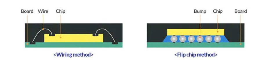
The base material of IC packages is the integrated circuit substrate (or IC package substrate). They shield the bare IC while supporting interconnection between the IC and the PCB’s trace network. As a result, the substrate has a significant impact on circuit performance
By applying the guidelines in this article around stackup sequence, material selection, hole registration, panelization and thermal management, engineers can fully utilize 10 or more layers for their complex designs. Partnering with a shop experienced in high layer count boards ensures achieving the quality and functionality required to maximize your product’s capabilities and service life.