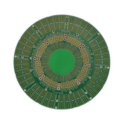
Radar PCBs are described as PCB substrates designed for radars. These PCBs are essential for communication circuits and detection. Radar PCBs use high-frequency PCB materials. Since they are used for communication and detection circuits, radar PCBs need to be highly efficient and operate at higher frequency outputs than standard PCBs. They are designed to send and receive radio frequency signals.
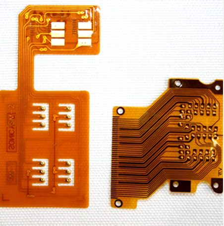
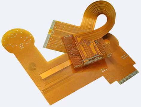
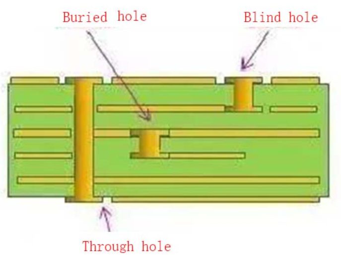
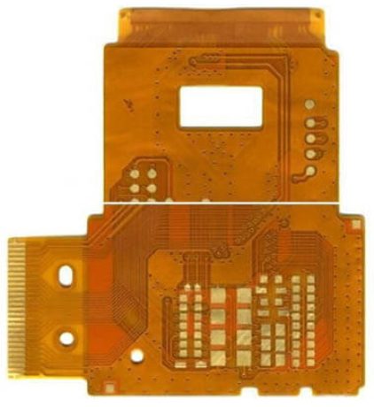
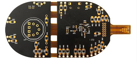
Flexible PCB is a unique type of printed circuit board that replaces the rigid FR4/metal/PTFE/ceramic substrate with a thin, bendable polyimide (PI) substrate and replaces the solder mask with a PI coverlay. Plated through holes or buried vias insulate and protect the conductive copper traces that connect the various flexible PCB layers to the non-conductive PI material. Flexible circuit board, flexible PCB or FPC is another name for flexible PCB.
China, as the world’s largest automotive market, has positioned itself as a formidable force in the field of autonomous driving technology. With over 160 OEM manufacturers and a rapidly growing electric vehicle (EV) sector, the nation’s drive toward intelligent mobility is accelerating. This blog explores the current state of autonomous driving technology in China, highlighting key players, technological advancements, and the unique strengths that position China as a global leader in this field.
FPC flexible PCB boards can produce four-layer PCB boards, but compared to double-layer or multi-layer FPC flexible PCB boards, the manufacturing process is more complex and issues such as insulation performance, signal transmission, manufacturing processes and applications need to be considered.
A via is a small hole on a PCB that connects different layers electrically. Structurally, a via consists of a drill hole and a pad.
Single-sided and double-sided PCBs serve different purposes based on complexity and application needs. Single-sided PCBs are cost-effective and ideal for simpler designs, while double-sided PCBs provide flexibility and higher circuit density for advanced devices.
Flexible printed circuit boards (FPCBs) are essential components in modern electronic devices, offering versatility, lightweight design, and the ability to adapt to a variety of shapes. The manufacturing process of flexible PCBs involves several key steps, each of which is critical to ensuring the quality and performance of the final product.
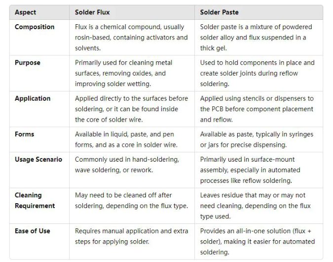
Soldering is a critical process in electronics and metalworking that is used to connect components by melting filler metal, or solder, to form reliable electrical and mechanical connections. Two key materials that assist in this process are flux and solder paste.
Special process flow for PCB processing of circuit boards As a practitioner in the PCB industry, for PCB copying, PCB design-related processes must be mastered.
As a PCB designer or manufacturer, you are constantly challenged with how to achieve better results. You want to provide new solutions or breakthroughs to problems. In some cases, these problems may require new features. It can also be a choice between module-based or custom PCB design. In any of these cases, you need a special PCB type. The growing demand for electronic functions such as high speed or high power in odd spaces makes special circuit board types essential.

