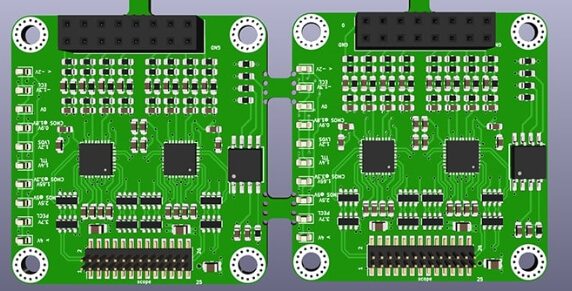
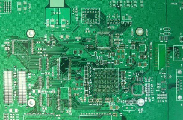
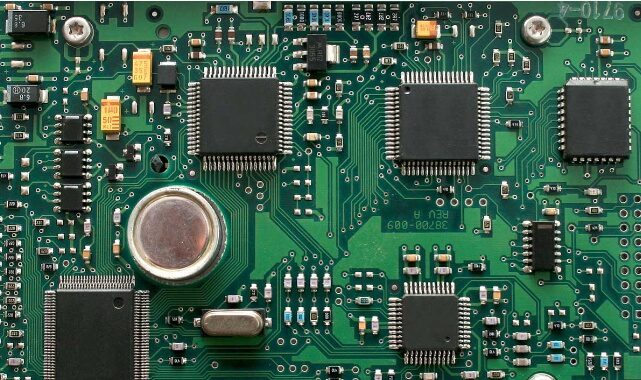
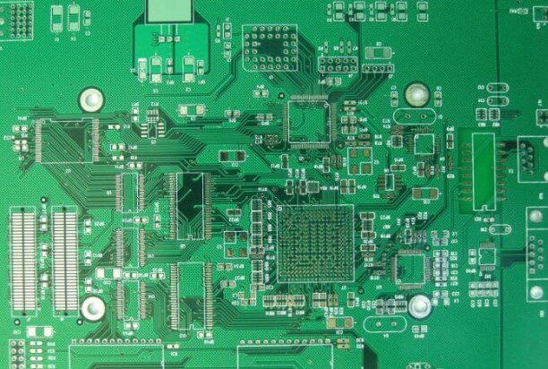
When designing high-speed PCBs, process variations and other factors can significantly impact actual impedance. Automated design tools may not always detect these subtleties, making proactive, defensive design essential. Here’s how to address common challenges in high-speed PCB design.
To ensure high-quality signal transmission and reliability in high-frequency PCB designs, adhering to effective wiring strategies is essential. Here are optimized guidelines and techniques, with key points highlighted for easy reference:
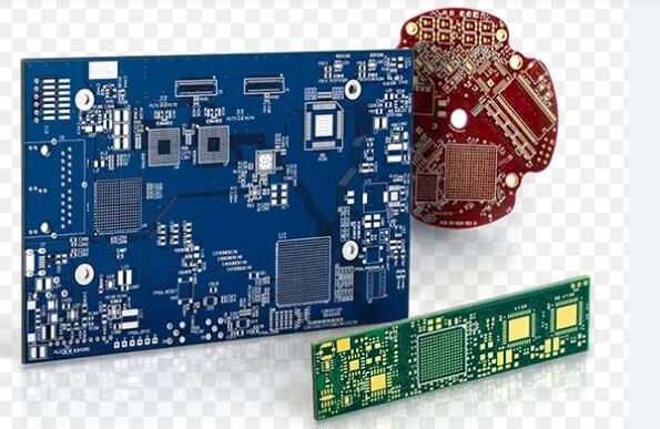
In today’s technology-driven world, the Printed Circuit Board (PCB) stands as a foundational component in electronic devices. From smartphones to complex medical equipment, PCBs are essential for ensuring reliable electrical connections and functionality. This article delves into the critical stages of PCB design, manufacturing, and final artwork, providing insights into the complexities and technicalities of creating effective circuit boards.
Multilayer PCB design follows principles similar to double-layer design, with added structural complexity and a focus on stable signal integrity and efficient routing. With experience in double-layer PCBs, moving to multilayer designs can be manageable.
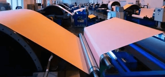
In the PCB industry, the common types of copper foil are Rolled Annealed Copper (RA) and Electrodeposited Copper (ED).
Following these practical tips for high-frequency PCB design helps in optimizing interconnections within the board. Techniques such as using 45° transmission lines, precision etching, and non-leaded components will significantly enhance circuit performance. Familiarizing yourself with these methods makes designs like back-copper coplanar microstrip layouts both economical and efficient.
RF circuit board design is a critical and often complex area of PCB engineering. While there are many uncertainties in theory, practical design rules can be followed to optimize performance.
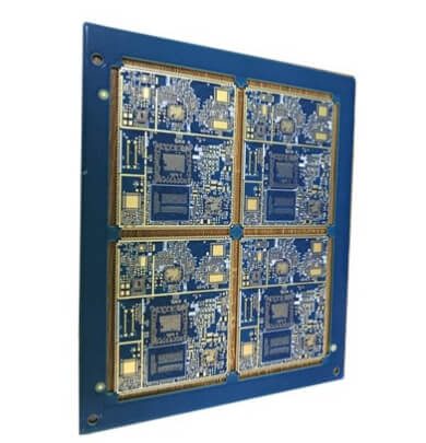
HDI boards represent the forefront of PCB technology, enabling smaller, more efficient electronic devices while meeting the demands of modern consumer electronics and telecommunications.
Printed Circuit Boards (PCBs) are the foundation of most electronic devices. The PCB production process can be categorized into subtractive methods and additive methods. Currently, the most commonly used industrial method is the copper foil etching process, a subtractive method.
HDI board is the abbreviation of High Density Inverter. It is a kind of (technology) for producing printed circuit boards. It is a circuit board with relatively high line distribution density using micro blind buried hole technology. HDI board is a compact product designed for small-capacity users. It adopts modular parallel design. One module has a capacity of 1000VA (height 1U), natural cooling, and can be directly placed in a 19″ rack. Up to 6 modules can be connected in parallel. This product adopts full digital signal process control (DSP) technology and multiple patented technologies. It has full range of load adaptability and strong short-term overload capacity, and can ignore the load power factor and peak factor.
In fact, there is no clear definition of HDI high-density manufacturing method, but generally there is a big difference between HDI and non-HDI. First of all, the aperture used in the circuit carrier made of HDI must be less than or equal to 6mil (1/1,000 inch), and the ring diameter of the hole ring must be ≦10mil, and the layout density of the line contacts must be greater than 130 points per square inch, and the line spacing of the signal line must be less than 3mil.


