


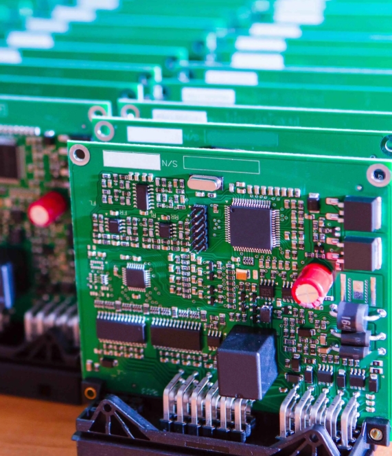
1. Background Overview Under the accelerating global trend of industrial automation, a client from Europe aimed to develop a servo drive product with high dynamic response, high-precision control, and high integration for their next-generation industrial automation equipment. After evaluating multiple suppliers, the client ultimately chose to collaborate with KKPCB, seeking a one-stop customized service from […]
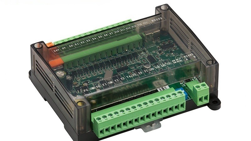
1️⃣ Background Overview With the tightening of global environmental regulations and the upgrading of industrial water resource management needs, sewage treatment plants of customers in Europe, America and the Middle East are in urgent need of highly reliable and extreme environment resistant automation control systems. Traditional PLC modules have pain points such as frequent signal […]

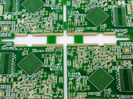
The customer is a globally leading manufacturer of communication equipment, specializing in the development and production of large-scale routers, switches, servers, and high-speed networking devices. As modern network communications demand increasingly high signal integrity, reliability, and thermal stability, the customer required an 18-layer PCB with low-loss material (S1000-2M) and advanced immersion gold plating to ensure stable signal transmission and long-term reliability
When designing a PCB, one of the critical decisions you’ll face is whether to use plated or unplated mounting holes. These holes are essential for securing the PCB to an enclosure or package, but the choice between plated and unplated holes depends on your design requirements, grounding needs, and mechanical considerations. Let’s explore the differences, advantages, and best practices for each type.
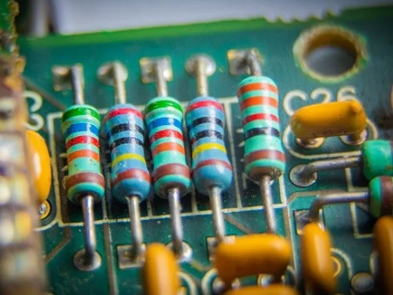
PCB resistors are designed to be mounted and soldered to printed circuit boards; they control current flow and divide voltages, among other things. PCB resistors come in many shapes and sizes, but they’re all designed to fit easily into board layouts. They have two terminals that can be soldered to the conductive traces on the PCB so they can be connected electrically to the rest of the circuit.
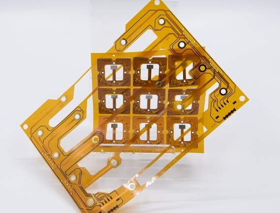
It wasn’t long ago that rigid circuit boards were the only possible electronic system method available. Whether it was entertainment or industrious, the shape of most devices was an extension of an intractable rigid board. More recently, the tide has turned: as technology has developed and matured, the enclosure is shaping the electronics inside them. Despite additional manufacturing challenges, flexible PCBs (or flex printed circuits) are enticing to product designers due to a nearly unlimited range of possibilities compared to rigid board constraints.
PCB routing involves laying out traces to minimize interference, ensure signal integrity, and meet design requirements such as impedance control and thermal management. Traces carry electrical signals between components such as integrated circuits, resistors, and capacitors. PCB traces are usually made of copper.
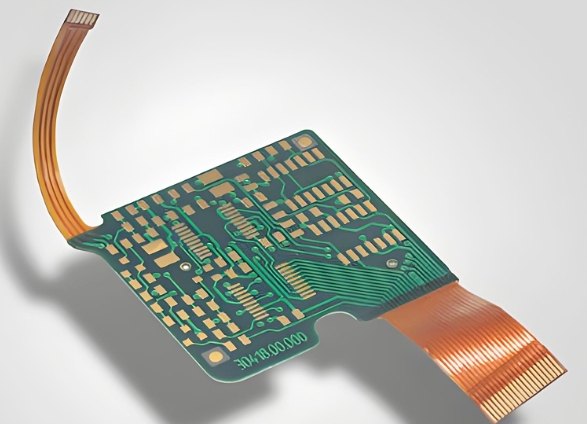
Combining the flexibility of flex circuits with the robustness of rigid boards, while leveraging High-Density Interconnect (HDI) technology, represents a significant breakthrough in modern electronics. Traditional methods like board-to-board stacking connectors or standard flex circuits often present challenges, such as cumbersome assembly and potential damage during connection. Rigid-flex PCBs offer a seamless solution, eliminating these bottlenecks and enabling more efficient designs.
These PCB tolerances ensure that PCB circuit boards are produced precisely and can function as intended. Manufacturers adhere to specific in-house tolerance guidelines, based on international standards like IPC-A-600 Class 2, to maintain quality throughout the production process.
When designing for PCB prototyping, the cost of individual parts does not always play a big role. If you’re designing one-offs or hobby projects, you’ll probably only look at parts prices when your assembly house sends you an invoice.