


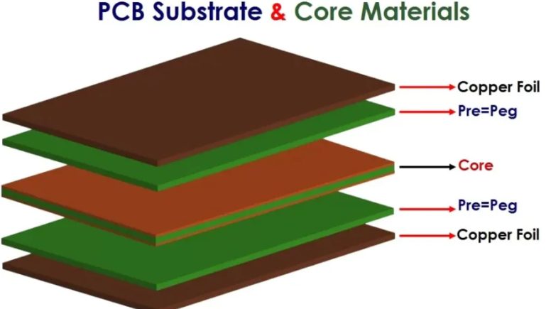
The Printed Circuit Board (PCB) is a fundamental component in all modern electronics, providing the platform for the electronic components and circuits. The performance, durability, and overall quality of a PCB are heavily influenced by the materials used for its substrate and core. This comprehensive guide explores the different types of PCB substrate and core materials, their properties, applications, and why they are important for engineers, PCB manufacturers, and students.
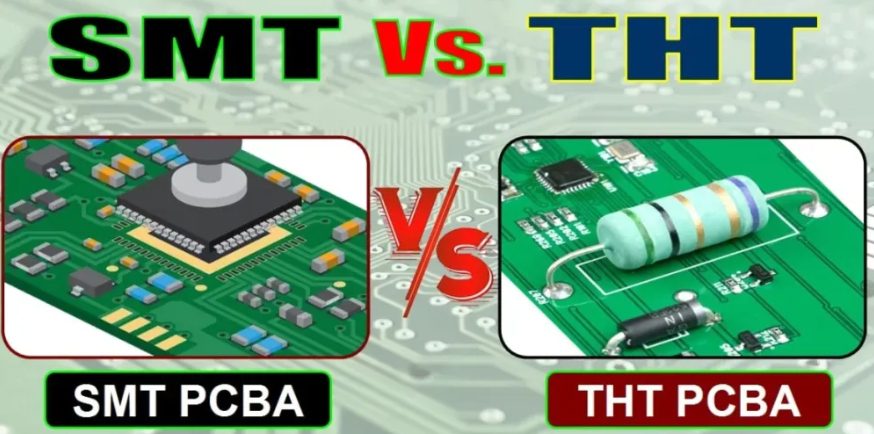
Surface Mount Technology (SMT) and Through-Hole Technology (THT) are two key PCB assembly methods widely used in electronics manufacturing. Both technologies have their own distinct advantages, applications, and processes. In this article, we will explore the differences between SMT and THT, examining the assembly steps, key features, and when each technology is ideal for use.
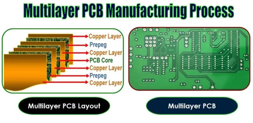
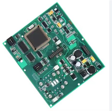
A multilayer PCB is a printed circuit board that consists of more than two layers, typically at least three or more layers of conductive copper, separated by an insulating material (substrate). These layers are stacked and connected by vias, resulting in a compact and efficient PCB design.
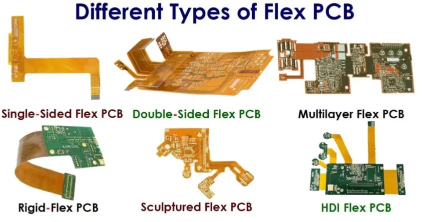
A flexible printed circuit board (FPCB) is a type of PCB that can be bent or twisted to fit into specific spaces or conform to different shapes. Unlike rigid PCBs, FPCBs are made from flexible materials, such as polyimide, and are ideal for use in compact, complex, and high-performance electronic devices.
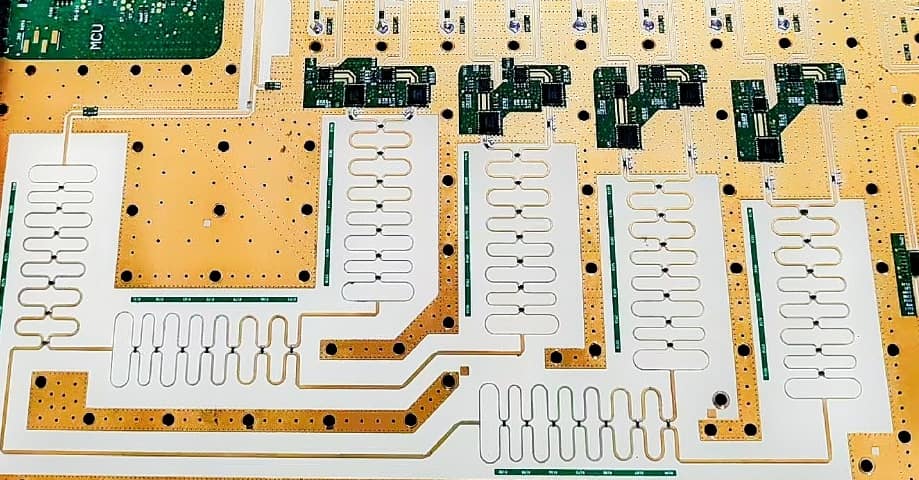
Advanced PCBs are complex multi-layer printed circuit boards (PCBs) with significantly more layers than standard multi-layer boards. These advanced PCBs are crucial for high-end, high-precision electronic devices, which are typically found in industries like industrial equipment, instrumentation, automotive electronics, aviation, military applications, communication systems, complex computing, and space technology.
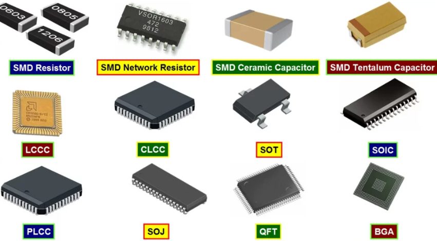
SMD (Surface-Mount Device) components and SMT (Surface-Mount Technology) stickers serve the same electrical functions. However, due to their small size, SMD components offer better electrical performance. Despite these advantages, not all components are available for surface mounting. High-end processors and large connectors like BGAs (Ball Grid Arrays) and PGAs (Pin Grid Arrays) often require mixed assembly modes due to their unique requirements.
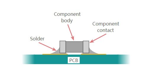
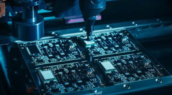
Surface Mount Technology (SMT) has revolutionized the electronics industry by enabling compact, efficient, and cost-effective PCB assembly. Today, nearly all commercially manufactured electronic devices utilize SMT for its ability to pack more functionality into smaller spaces and improve manufacturing processes through automation.
When assembling a printed circuit board (PCB), components are mounted onto the board through one of two primary methods: Surface Mount Technology (SMT) or Through-Hole Technology (THT). Each method has distinct advantages and is suited to different applications depending on the project requirements.
There are three main sources of heat in PCB: heat from electronic components; heat from PCB itself; Heat from other parts.
Among the three heat sources, the heating from electronic components is the largest, followed by the heat generated by PCB board, and other heat from the outside based on the overall thermal design of the system.
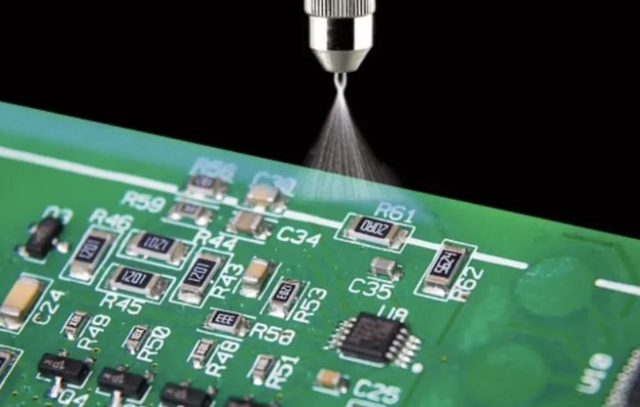
Conformal coatings play a critical role in ensuring the longevity and reliability of printed circuit boards (PCBs). Whether designing electronics for consumer devices, automotive systems, or military applications, selecting the right conformal coating is essential.