


1. Background Overview Under the accelerating global trend of industrial automation, a client from Europe aimed to develop a servo drive product with high dynamic response, high-precision control, and high integration for their next-generation industrial automation equipment. After evaluating multiple suppliers, the client ultimately chose to collaborate with KKPCB, seeking a one-stop customized service from […]
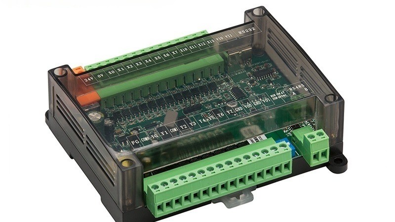
1️⃣ Background Overview With the tightening of global environmental regulations and the upgrading of industrial water resource management needs, sewage treatment plants of customers in Europe, America and the Middle East are in urgent need of highly reliable and extreme environment resistant automation control systems. Traditional PLC modules have pain points such as frequent signal […]

The customer is a globally leading manufacturer of communication equipment, specializing in the development and production of large-scale routers, switches, servers, and high-speed networking devices. As modern network communications demand increasingly high signal integrity, reliability, and thermal stability, the customer required an 18-layer PCB with low-loss material (S1000-2M) and advanced immersion gold plating to ensure stable signal transmission and long-term reliability
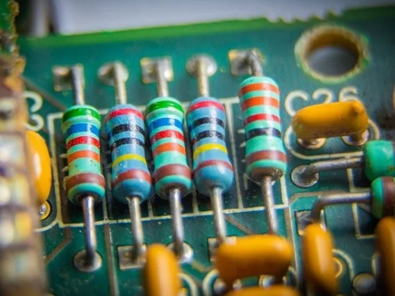
PCB resistors are designed to be mounted and soldered to printed circuit boards; they control current flow and divide voltages, among other things. PCB resistors come in many shapes and sizes, but they’re all designed to fit easily into board layouts. They have two terminals that can be soldered to the conductive traces on the PCB so they can be connected electrically to the rest of the circuit.
Electronics are becoming faster, smaller, and used in more demanding environments. Miniaturized ICs and SMDs operate at higher frequencies and require more power. Increased current demands cause voltage drops across resistive elements, generating heat and leading to temperature rises and hotspots. Over half of electronic component failures now stem from heat-related stress.
Printed Circuit Board (PCB) routing is a critical aspect of electronic design, ensuring that electrical signals are transmitted efficiently and reliably between components. Proper routing minimizes interference, maintains signal integrity, and meets design requirements such as impedance control and thermal management. This article outlines the best practices for PCB routing, focusing on optimizing performance and ensuring signal integrity.
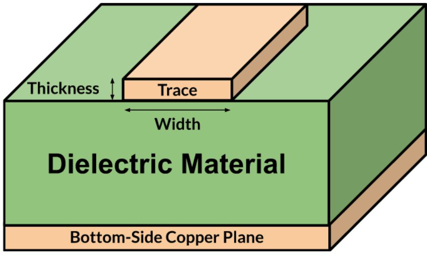
The relationship between PCB trace thickness and current capacity is a critical aspect of PCB design. Properly sizing traces ensures that they can handle the required current without overheating, which is essential for the reliability and functionality of the circuit. This article explores the key considerations for selecting trace thickness, the impact of copper weight, and methods for calculating current capacity, along with design strategies for high-current applications
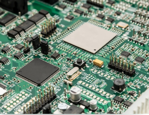
Creating a robust component library is one of the most challenging yet critical aspects of PCB design. The quality of the library, which includes schematic symbols, PCB footprints, and 3D models, directly impacts the success of your board development. Among these, the PCB footprint plays a pivotal role in determining whether your board can be manufactured and assembled correctly.
Unlike fixed power supplies that provide a constant output voltage, variable power supplies can be adjusted to different output voltages as needed. In contrast, fixed voltage power supplies or battery chargers provide a single, unchanging output voltage and are designed for specific, consistent power requirements. Read on as we discuss variable power supply PCB layout tips.
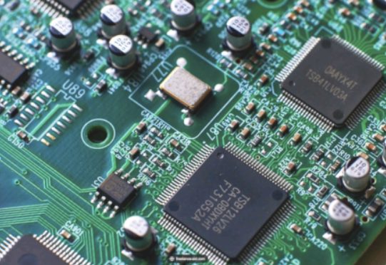
In high-speed and RF PCB designs, controlling trace impedance is critical, but the role of RF via transitions is often underestimated. Vias, which connect signals between layers, can introduce impedance mismatches, signal reflections, and losses, especially at high frequencies. Proper design and optimization of via transitions are essential to maintain signal integrity and ensure reliable performance in RF and high-speed digital applications